Continue to Site

Welcome to EDAboard.com

Welcome to our site! EDAboard.com is an international Electronics Discussion Forum focused on EDA software, circuits, schematics, books, theory, papers, asic, pld, 8051, DSP, Network, RF, Analog Design, PCB, Service Manuals... and a whole lot more! To participate you need to register. Registration is free. Click here to register now.

[SOLVED] Switching power supply TOP246 - primary snubber diode fail

Status
Not open for further replies.

1.5kV

Newbie level 4
Joined
Dec 13, 2016
Messages
6
Helped
0
Reputation
0
Reaction score
0
Trophy points
1
Activity points
55
Hello everybody,

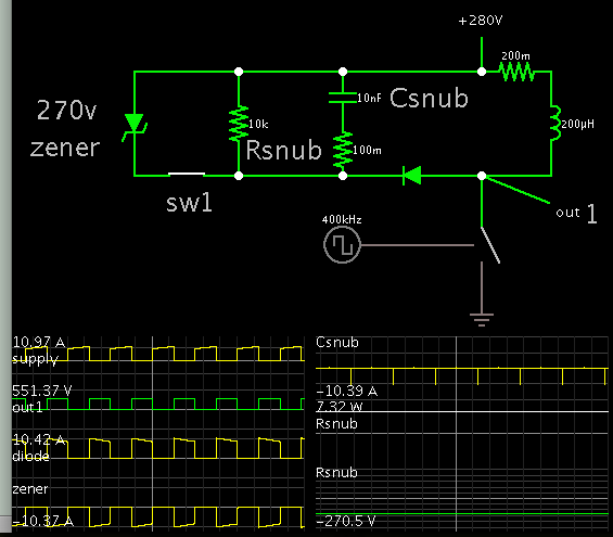
I have an interesting situation with a failing diode D1 in the snubber of a switching power supply. According to the diode specification and the design of the snubber I can't imagine what could possibly damage the diode.

Any hints will be greatly appreciated.

top246.png

Best regards
 

what is your transformer specification?
 

Your transformer construction may not be optimal, thus having more leakage inductance than what the snubber was designed to cope with.
 

The capacitor C6 charges through the diode immediately as the transformer is turned Off. Then the capacitor loses charge through the resistors during the remainder of the cycle. There needs to be a balance in the give-and-take, so that the capacitor charge stays in a manageable range.

Human nature would tend to make C small, R large. Unfortunately this may result in the capacitor charging to a very high voltage. If it rises higher than the diode is rated for, it destroys the diode.
 

Thanks for your quick response.

Ok let's make some conclusions..

If I understand correctly there are two scenarios where the diode gets shorted:
1. Reverse overvoltage
2. Too high forward current

1. Is probably not likely to happen because capacitor can't charge to higher than 200V +/- tolerance because of clamp diode VR1. Only if clamp diode would react too slow when the voltage goes above breakdown voltage...
2. This could be the consequence of the higher leakage inductance of the transformer than the snubber is designed for?

So far I haven't measured the leakage inductance yet - I know, that would be the first thing that i should do :)

Thanks for the tips so far. I will measure the leakage inductance and calculate if the snubber design is sufficent or not. If in the mean time you get any other idea please don't hesitate to tell it.

Best regards
 

Would like to see the circuit layout. Most likely diodes fail due to overvoltage during commutation. This might happen if there's excessive wiring inductance in the commutation loop (C1-C6-D1-U1).
 

Hi FvM,

Here is the layout:
**broken link removed**
 

1. Is probably not likely to happen because capacitor can't charge to higher than 200V +/- tolerance because of clamp diode VR1. Only if clamp diode would react too slow when the voltage goes above breakdown voltage...

Your schematic shows the supply voltage 250-380V. Since this is greater than 200V, it effectively puts a freewheeling diode across the inductor. This should not be done in a flyback. After all, if a simple diode were sufficient to use in a flyback, there would be no need for an elaborate snubber network. (Although a freewheeling diode is sufficient in other types of circuits). The zener diode passes current for part of the cycle, and then it also allows current to continue circulating around a loop for a longer time than it ought to. Current can build from one cycle to the next. Power is wasted going around the primary loop, instead of going to the secondary winding.

My simulation shows current building to many times the original amount. (I assume 1 or 2 Amps is the intended amount, since output power is listed as 250W.) My zener is 270V which is 10V less than the supply V.


It might be safe to use a zener value which is equal to the supply V. Even so, the C & R values ought to be adjusted so they are able to dissipate the energy coming from the transformer at shut-off, from one cycle to the next.
 

Here is the layout again
03_TOP246_layout.png

- - - Updated - - -

BradtheRad I am not sure if I understand you correctly. If there would be current flowing thru the zener VR1 and D1 then the zener would be destroyed before D1. Power on zener is 200V*current, power on D1 is 0,7V*same current. Probably I didn't understand correctly.
 

So far I haven't measured the leakage inductance yet - I know, that would be the first thing that i should do :)

I am still leaning towards a problem in the transformer design or construction.
 

BradtheRad I am not sure if I understand you correctly. If there would be current flowing thru the zener VR1 and D1 then the zener would be destroyed before D1. Power on zener is 200V*current, power on D1 is 0,7V*same current. Probably I didn't understand correctly.

Admittedly my simulation cannot duplicate your real flyback hardware. It's likely you don't have the large 'theoretical' current as my simulation shows. Nevertheless it reveals how the action is similar to a freewheeling diode, so it could create the same problem as a freewheeling diode.

There is the other issue of reverse voltage (mentioned previously). Notice the diode is exposed to the sum of supply V plus capacitor V. However you might have momentary spikes which exceed that, if the capacitor has significant ESR, and the zener is slow to conduct.
 

Can you be more specific about the Line/Load conditions under which the circuit fails? Does D1 gradually heat up before failing, or is does it die immediately when those conditions are applied, regardless of temperature? This would help narrow down whether the issue is excessive conduction current or reverse voltage (or both).
 

The BYV26C is notorious for breaking down (from over heat) under high frequency hard reverse recovery (380V in this case) - if you put a thermo-couple on it and start the converter you will see its temp go up until it fails - chose a better diode with <35nS reverse recovery..!
 
Is C1 22 µF? How long are it's terminal wires.

Actually I put 82uF inside. Terminal wires are short, just thickness of the PCB (63 mils).

- - - Updated - - -

Can you be more specific about the Line/Load conditions under which the circuit fails? Does D1 gradually heat up before failing, or is does it die immediately when those conditions are applied, regardless of temperature? This would help narrow down whether the issue is excessive conduction current or reverse voltage (or both).

Hi mtwieg,
I can confirm that when the diode fails there are also seen signs of excessive heat. Still didn't calculated the snubber design yet...

- - - Updated - - -

The BYV26C is notorious for breaking down (from over heat) under high frequency hard reverse recovery (380V in this case) - if you put a thermo-couple on it and start the converter you will see its temp go up until it fails - chose a better diode with <35nS reverse recovery..!

Ok thanks, that is interesting...
 

Everything looks like there was an issue with diode reverse recovery time. The snubber design seems to be fine - i checked the leakage inductance, did the calculations for the snubber and checked Vds voltage.
Thanks to all for constructive thoughts and of course big thanks to Easy peasy.
 

Status
Not open for further replies.

Similar threads

Part and Inventory Search

Welcome to EDABoard.com

Sponsor

Back
Top