Continue to Site

Welcome to EDAboard.com

Welcome to our site! EDAboard.com is an international Electronics Discussion Forum focused on EDA software, circuits, schematics, books, theory, papers, asic, pld, 8051, DSP, Network, RF, Analog Design, PCB, Service Manuals... and a whole lot more! To participate you need to register. Registration is free. Click here to register now.

Simulating CMOS Ring Oscillator in AWR AO at the desired bias voltage

Status
Not open for further replies.

cannibol_90

Member level 5
Joined
Jun 20, 2009
Messages
83
Helped
5
Reputation
10
Reaction score
5
Trophy points
1,288
Activity points
2,066
Hi, :)

We are trying to simulate a CMOS Ring Oscillator using AWR AO. We are amateurs and only know the basic design equations for designing one.

We are using 180nm technology and the maximum VDD allowed is 1.8V (as said by our boss). But the problem is that we are getting oscillations only at approximately 5V bias.

No matter how much we change the widths and lengths the oscillations occur only at a bias voltage of 5V. We are using BSIM3 version for the NMOS and PMOS. We understand that the problem is with the MOSFET model used.

We tried the AWR example of Push Push Oscillator and the output was obtained beautifully at the desired voltage.

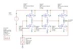
Please help us in understanding what parameters or model of the MOSFET has to be changed so as to obtain an output at the desired voltage. We are attaching the schematic and simulated results.

Please Help!

ring oscillator 5V.jpg
ring oscillator 5V output.jpg
ring oscillator 1.8V output.jpg
 

Attachments

  • VCO.7z
    23.2 KB · Views: 137

I don't know the AWR AO tool, sorry.

Does your CMOS Ring Oscillator use the same MOSFET models (BSIM3V322(P)) as the "Push Push" Oscillator example?
 
The circuit appears to go into stagnant mode. The output meanders in a middle voltage range, rather than a definite on-or-off condition.

Can you set the very first input to low or high initially? Or connect it briefly to a supply lead as you start up?
 

Does your CMOS Ring Oscillator use the same MOSFET models (BSIM3V322(P)) as the "Push Push" Oscillator example?

You guessed it ;). NO, I don't! There is a reason for that. First of all, the Ring Oscillator given in the AWR example is Ring_Oscillator_Extraction and not Push Push oscillator (yes, it is Push Push and not Push Pull).

The MOSFET Model used in the AWR AO example is Gen:Bic35 model. It is said in the design notes that: "In this example, the STACKUP element is located in the “Global Definitions” section. The STACKUP element must be located either in the “Global Definitions” or in the same schematic as the EXTRACT block. The settings for the STACKUP element are beyond this example since this block is typically fixed per PDK and provided with the PDK being used."

Now, in this model, the widths and lengths can be adjusted accordingly. But, there are predefined lower and upper limits. The lower limit for the length is 0.35um. Therein lies the problem. We need a length of 0.18um or 180nm!

- - - Updated - - -

The circuit appears to go into stagnant mode. The output meanders in a middle voltage range, rather than a definite on-or-off condition.

Can you set the very first input to low or high initially? Or connect it briefly to a supply lead as you start up?

I don't understand by "setting first input to low or high". Do you mean the first CMOS inverter? What is a "supply lead"? And which is the corresponding element in AWR? Thanks for the reply! :)
 

We understood that the problem is with the unavailability of the PDK for 0.18um process. The Generic GenBicmos35 PDK uses a channel length of 0.35um. Are there any PDKs of 0.18um available for free download?
 

We understood that the problem is with the unavailability of the PDK for 0.18um process. The Generic GenBicmos35 PDK uses a channel length of 0.35um. Are there any PDKs of 0.18um available for free download?

You can get PDKs only from the foundries or their representatives against signing an NDA (s. here), or GPDKs from the EDA tool companies.

But I guess you just need appropriate model files for a 0.18µm process. Why not use the free PTM models? Click Latest Models, then scroll down to the bottom, where you still can find 180nm BSIM3 level=49 NMOS & PMOS SPICE models.
 
Last edited by a moderator:
You can get PDKs only from the foundries or their representatives against signing an NDA (s. here), or GPDKs from the EDA tool companies.

YES! There are some NDA to be cleared from Towerjazz (Foundry) and AWR before the PDK reaches our hands.

But I guess you just need appropriate model files for a 0.18µm process. Why not use the free PTM models? Click Latest Models, then scroll down to the bottom, where you still can find 180nm BSIM3 level=49 NMOS & PMOS SPICE models.

Wow 8-O! Thanks a lot Erikl :thumbsup:! I don't see any model, but only the parameters. Is there any way to export all the parameters at once into the model, instead of manually one by one?
 
Last edited:

I don't see any model, but only the parameters. Is there any way to export all the parameters at once into the model, instead of manually one by one?

These are models:


Code PHP (brief) - [expand]
1
2
3
4
5
6
7
*
* Predictive Technology Model Beta Version
* 180nm NMOS SPICE Parametersv (normal one)
*
 
.model NMOS NMOS
+Level = 49


You .include them by their path (or copy/paste them) into your control file, then call (instantiate) the FETs with their names, referring to the models (NMOS or PMOS), adding their W & L parameter values. See your simulator instructions how to do this (as mentioned, I don't know the AWR sim.).

Usually like this example:
x1 drain gate source substrate NMOS W=1e-6 L=180n * x1 is the individual FET's name; NMOS refers to the model.
 
The output was not obtained by PTM 0.18um model but by the TSMC 180nm model for level 49. The PTM 0.18um model shows some translational errors. :sad:

We imported the model parameters to NETLIST, drew a sub-circuit and added a symbol for the MOSFET. The model is working well for a bias voltage of 1.5V! :grin:

Now the problem is how to adjust its width. How to make the model's length and width as variables?

https://awrcorp.com/download/faq/english/docs/Users_Guide/importing_netlists.html

1.jpg
2.jpg
3.jpg
4.jpg
5.jpg
 

Attachments

  • MOSFET Netlist Working.7z
    14.2 KB · Views: 126
Last edited:

Now the problem is how to adjust its width. How to make the model's length and width as variables?

Usually in (H)SPICE simulators you can assign a parameter (e.g. wn, ln for NMOS), give it a preliminary value, and in the analysis sweep it between limit values:
.DC sweep wn LIN 10 0.1u 1u

Some simulators can sweep multiple parameters, HSPICE e.g. with the DATA structure.

This tutorial shows how it's done with the Cādence tool (s. pp. 15 ff): View attachment Cadence_tutorial_parametric_analysis.pdf
 
Usually in (H)SPICE simulators you can assign a parameter (e.g. wn, ln for NMOS), give it a preliminary value, and in the analysis sweep it between limit values:


Some simulators can sweep multiple parameters, HSPICE e.g. with the DATA structure.

This tutorial shows how it's done with the Cādence tool (s. pp. 15 ff): View attachment 120285

We don't know how to perform a sweep for a variable inside the NETLIST. A parameter sweep in AWR can be done only if the variable is accessible. https://awrcorp.com/download/faq/english/docs/Simulation/sa_basics.html#swept_parm

Instead we added .SUBCKT command to the NETLIST file. Now the width and length is accessible and they can be varied. https://awrcorp.com/download/faq/english/docs/Users_Guide/importing_netlists.html
Spice.jpg

The ring oscillator output at a Bias voltage of 1.5V:
ring.jpgring output.jpg

Now certain questions pops up in my mind.

1. Which parameter in this model file corresponds to the length and width of the MOSFET? In case it is not there, how to calculate it? We need the minimum and maximum length and width for simulation purposes.

2. How to verify this model is for 180nm technology?

3. Can the parameters in the model be changed for a low voltage/power consumption?
 

Instead we added .SUBCKT command to the NETLIST file. Now the width and length is accessible and they can be varied.
Well done, congrats! The .SUBCKT + M1 method is only necessary for the sweep, not for building a netlist. For a netlist without sweeping parameters, you could assign the width and length for individual transistors directly:
MS1 1 2 3 4 CMOSN W=1u L=0.18u
MS2 1 2 5 5 CMOSP W=3u L=0.18u
. . .


1. Which parameter in this model file corresponds to the length and width of the MOSFET? In case it is not there, how to calculate it? We need the minimum and maximum length and width for simulation purposes.
The original model file doesn't contain parameters for W & L , but it's necessary to assign these values for each individual transistor, s. above (or with your .SUBCKT method for sweeping).

2. How to verify this model is for 180nm technology?
T92Y was a (6 years old) TSMC 0.18µm wafer lot, these data had been published freely by MOSIS in former days (still in 2015, AFAIR).
Without knowing this, you can judge the process size from the thin gate oxide parameter TOX, which is 4.1nm in your CMOSN model file, a typical value for a 0.18µm process.

3. Can the parameters in the model be changed for a low voltage/power consumption?
You don't change parameters of a model file - apart from W & L - because this foundry-provided model description describes how their MOSFET will behave, and this is what you want to see by simulation - and later in reality, perhaps.

Changes of power consumption can only be realized by changes of your netlist, i.e. changes of W, L, power supply voltage, frequency ...
You'll get min. power consumption with lowest possible W & L values (0.18µm in your case) and lowest possible power supply voltage - as long as the circuit will still start oscillating - and this should be checked for all worst case conditions in PVT (process, voltage, temperature).
 
Sir,

1. But what can be the min. and max. widths and lengths that can be specified for this model? Or is it an ideal model?
Does LINT and WINT specify the initial lengths and widths?

2.
You don't change parameters of a model file - apart from W & L - because this foundry-provided model description describes how their MOSFET will behave, and this is what you want to see by simulation - and later in reality, perhaps.

OMG! So do you mean that when we receive our PDK from TowerJazz, and in case it is different from the parameters that we are using, the output would be different, right? But we are training ourselves on using AWR AO, design/modify CS-VCO for low power consumption, low phase nose et al. We have seen certain authors adding linearizing Resistors, MOSFETS, capacitors etc. for improved design. Any suggestions/advices/comments from your side, sir?

3. cs-vco W=3um L=180nm.jpg
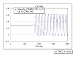
For the CS-VCO attached above, we used a width of 3um for all transistors and a length of 180nm. The output oscillations can be obtained with a bias voltage as low as 0.6V (control voltage being 0.4V), but the delay is observed to be as high as 900ns approximately. It this acceptable? What is the maximum allowed delay?
cs vco high delay.jpg

4. Also, 180nm means that the maximum bias voltage that can be applied is 1.8V, right? Does it mean that 1.8V is the maximum voltage that can be applied at Gate, Drain or Source?

5. What is the threshold voltage for this MOSFET? Is it VTH0? From the simulation it can be seen that the threshold is around 0.5V. But, VTH0 is given as 0.369V.
id vs Vgs.jpg
 
Last edited:

1. Min. specified length corresponds to the process size, same for min. width (in principle), but some foundries specify min. width > process size.
Max. length & width are unlimited (in principle, again), but foundries sometimes limit them to values around 10 .. 20µm, in order to be able to guarantee their model accuracy. Some foundries provide different models for different width ranges.

No, WINT & LINT are offset fitting parameters from I-V without bias for W & L, s. the BSIM3v3.2 Manual below, p. A-4.


2. Of course the models from a different foundry/fab will be different - but probably not as much as this would mean a full redesign. Your ring-oscillator probably will work with the same netlist. Just work with your TSMC models as long as you don't have the TowerJazz models available, after that simply exchange the models and see if you'd have to rework a bit.

3. This depends on your application.

4. This is correct, yes. But some processes have additional TOX options to allow for additional MOSFET models with higher supply voltages, like 3.3 or 5V, in order to allow for corresponding IO interfacing.

5. It's VTH0, right. Can be quite different for different processes, as the foundry can adjust VTH0 by implantations. Often they provide different VTH0 models with the same process (e.g. high VTH0 for min. power applications, and low VTH0 models for high speed applications).

VTH0 definition depends on several measurement conditions, as e.g. a fixed Ids measurement @ fixed Vds, and certain temperature, of course. See the BSIM3v3.2 Manual for definitions. It is possible that the resolution of your Ids vs. Vds plot isn't fine enough to reveal the model presented VTH0 value.
 

Attachments

  • BSIM3v3.2_MOSFET_MODEL.pdf
    5.1 MB · Views: 131
Status
Not open for further replies.

Part and Inventory Search

Welcome to EDABoard.com

Sponsor

Back
Top