Continue to Site

Welcome to EDAboard.com

Welcome to our site! EDAboard.com is an international Electronics Discussion Forum focused on EDA software, circuits, schematics, books, theory, papers, asic, pld, 8051, DSP, Network, RF, Analog Design, PCB, Service Manuals... and a whole lot more! To participate you need to register. Registration is free. Click here to register now.

clock buffer to be used for an external 1uF flying capacitor in a charge pump

Status
Not open for further replies.

allennlowaton

Full Member level 5
Joined
Oct 5, 2009
Messages
247
Helped
3
Reputation
6
Reaction score
3
Trophy points
1,298
Location
Taiwan
Activity points
3,061
Hello EDA fellows.
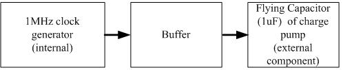
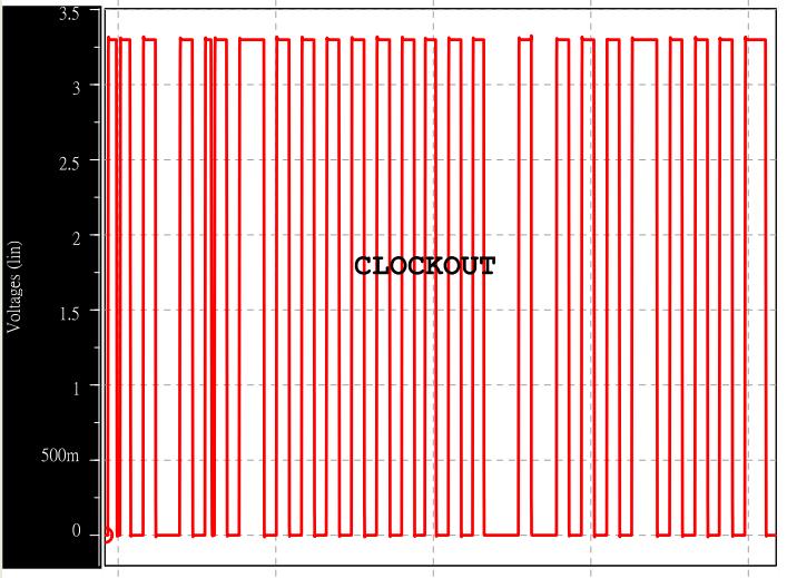
I want to ask you something about clock driving for my 1uF flying capacitor. I'm making my LED driver IC now and my problem is how can I drive my 1uF external capacitor with my internally produced 1MHz clock. I'm afraid taper buffer would be very very large if I'm going to use it.

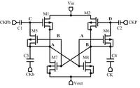
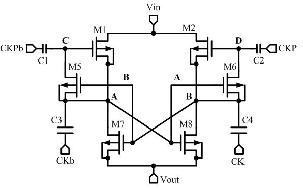
Below is the circuit diagram of my charge pump.


Thank you very much for your time.

Sincerely,

Allenn
 

Calculation is simple: I = 2fC*δV (factor of 2 , because you have only about half the clock cycle time for loading; δV is C's ripple). So with f=1e6 and C=1e-6 you get twice the voltage ripple as current. No pb. with milliVolts of ripple, but surely if you have to reload hundreds of milliVolts per cycle.
 
Hello Sir, Erikl...
Thank you very much for your reply..
I'm so sorry but I can't relate to your computation for the current. My concern is this, Is there any other option of clock buffer aside from the taper buffer that I could used for my internally produced clock pulses. I already have the circuit of the clock pulse generator and it works fine.

---------- Post added at 15:39 ---------- Previous post was at 15:34 ----------

Is the computed current is the amount of current that would flow through the inverter of the last stage of the taper buffer?
 

0_1305786481.jpg
 

Is the computed current .. the amount of current that would flow through the inverter of the last stage of the taper buffer?

Sure; the buffer should be capable of providing this current.
 
I'm a bit worried about the size of that taper buffer..I think it would be pretty big..Is there any other clock buffer that I can used?
 

Neither do I know your process nor the clock buffers of your library, sorry! But if the biggest one isn't big enough, you could probably use a few of them in parallel (use multiplicity factor m).
 
Sure; the buffer should be capable of providing this current.

the clock before without any buffer or load produced 1MHz. However, when the clock is connected to the pump through a 10 stages taper buffer the resulting frequency is not the same. I can't understand what just happened.
 

What's the frequency after buffer?
Pls use about 50% duty cycle clock for charge pump.
 
This is the simulation results of the clock generator + 10 stages buffer + Cload(47nF):


---------- Post added at 07:43 ---------- Previous post was at 07:32 ----------

This is the simulation results for the same clockout after it is being connected to the charge pump:


The waveform becomes irregular. The period decreased to 80ns from 1us.

I suspect the main culprit here is the OPTIONS that I had used. But I need to used them or else, "internal timestep problem" will occur.
 
Last edited:

Sometimes HSPICE shows internal timestep error, like internal timestep is too small. It is caused by convergence problem. You can try other simulator like Spectre.
Spectre's convergence is much better than HSPICE.
 
Sometimes HSPICE shows internal timestep error, like internal timestep is too small. It is caused by convergence problem. You can try other simulator like Spectre.
Spectre's convergence is much better than HSPICE.

That would be a big problem, I don't have Spectre.
 

I checked your waveform again. The first waveform shows another problem: The rising edge is much slow than falling edge. So driving capability in the buffer should be increased for this edge.
 
I checked your waveform again. The first waveform shows another problem: The rising edge is much slow than falling edge. So driving capability in the buffer should be increased for this edge.

I already increased the PMOS (with size 3 times as that of NMOS).
 

The actual ratio depends on process.
3 is just a reference value.
In some cases, larger number can be used.
 
Status
Not open for further replies.

Part and Inventory Search

Welcome to EDABoard.com

Sponsor

Back
Top