fanrong
Banned
Hi , everyone :
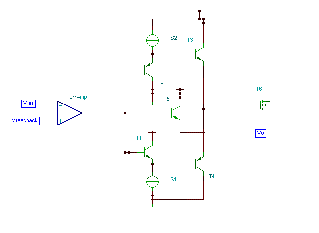
I draw a circuit of buffer for LDO. It is insert between the pass device
and the err amplifier to increase the pole to high frequency .The buffer is
coposed of T1 to T4 and Is1 Is2 . T5 is used to increase the speed of increaseing
the gate voltage of the pass device . It is like class-AB output stage of operational
ampliifer .
The buffer is in the graph below . Any advice or suggestion,such as how to
decrease the Iq , increase the speed , how to frequency compensation ......, will be appreciated .
Thanks forward !
Added after 1 minutes:
Added after 2 minutes:
Sorry , the graph is so small . so I post it's link :
https://obrazki.elektroda.pl/43_1174989203.gif