Continue to Site

Welcome to EDAboard.com

Welcome to our site! EDAboard.com is an international Electronics Discussion Forum focused on EDA software, circuits, schematics, books, theory, papers, asic, pld, 8051, DSP, Network, RF, Analog Design, PCB, Service Manuals... and a whole lot more! To participate you need to register. Registration is free. Click here to register now.

Strange behaviour from microcontroller pin

Status
Not open for further replies.
T

treez

Guest
Hello,

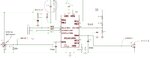
We are using the PIC16F18856 in 4x4mm UQFN package.

Port RA5 works when we program it as digital input…..reads it fine whether input is high or low. Port RA5 also works when we program it as digital output….gives a square wave output fine.

However, when we program the pin as an analog (ADC) input..it reads it but the 9th bit (dec 256) of the ADRES register is strangely always set high)….so for example even when we have a grounded input to the pin as an ADC, it reads 0x0100 instead of zero.

PIC16F18856 datasheet
https://www.microchip.com/wwwproducts/en/PIC16F18856
 

Hi,

I assume thus is no hardware problem

Does your code follow the ADC example given in the datasheet?

Klaus
 
  • Like
Reactions: treez

    T

    Points: 2
    Helpful Answer Positive Rating
Thanks, yes it does...on most of our boards, the ADC works fine. Its just around 30% of boards that are bad like this. Three out of ten...so we stopped production till we solve this.
The code is writen by a remote softy, but it looks bona fide.
Also, when we read ADC on RA4 pin it also has the same error on the bad boards.
We can shift the "bad bit" to the left with the left justify command, but its always in there.

Our ADC code is here, its just bog standard ADC code so i can post it here....

The errata says something which we dont fully understand so we are wondering and panicing about it..
Errata:
ww1.microchip.com/downloads/en/DeviceDoc/80000706B.pdf

Code:
//******************************************************************************
// Measure Light
//******************************************************************************
uint16_t MeasureLight(void)
{
    uint16_t  x;

    Init_Normal_ADC();
    ADC_StartConversion(0x05);          // Port A.5
    while (!ADC_IsConversionDone());
    x = ADC_GetConversionResult();
    return x;
}


//******************************************************************************
// The random.c DALI library change the ADC settings, so we need to restore them
// after a random command. Also this function initialize ADC the first time
//******************************************************************************


void Init_Normal_ADC()
{
       
    // ADGO stop; ADFM right; ADON enabled; ADCONT disabled; ADCS FOSC; 
    ADCON0 = 0x84;
    
    ADCON1 = 0x00;
    ADCON2 = 0x00;
    ADCON3 = 0x00;
    
    ADSTAT = 0x00;
    
    // ADCCS FOSC/2; 
    ADCLK = 0x00;  
    // ADNREF VSS; ADPREF VDD; 
    ADREF = 0x00;

    // CHANNEL --> ANA0; 
    ADPCH = 0x00;
    
    // PRECHARGE TIME -->  0; 
    ADPRE = 0x00;
    
    // ACQUISITION TIME --> 0; 
    ADACQ = 0x00;
     
    // ADDITIONAL CAPACITOR --> 0 
    ADCAP = 0x00;

    // AUTO conversion disabled; 
    ADACT = 0x00;
    
    
    // ADRPT 0; 
    ADRPT = 0x00;
    // ADLTHL 0; 
    ADLTHL = 0x00;
    // ADLTHH 0; 
    ADLTHH = 0x00;
    // ADUTHL 0; 
    ADUTHL = 0x00;
    // ADUTHH 0; 
    ADUTHH = 0x00;
    // ADSTPTL 0; 
    ADSTPTL = 0x00;
    // ADSTPTH 0; 
    ADSTPTH = 0x00;
    
      
    // ADC VALUE REGISTER L
    ADRESL = 0x00;
    // ADC VALUE REGISTER H
    ADRESH = 0x00;
}


//******************************************************************************
// Start ADC conversion
//******************************************************************************
void ADC_StartConversion(uint8_t channel)
{
    // Set CHANNEL
    ADPCH = channel;
    // ADRESL 0x0;
    ADRESL = 0x00;

    // ADRESH 0x0;
    ADRESH = 0x00;

    // Acquisition time delay
    __delay_us(ACQ_US_DELAY);

 
        // Turn on the ADC module
    ADCON0bits.ADON = 1;      

    // Start the conversion
    ADCON0bits.ADGO = 1;
}


//******************************************************************************
// Conversion DONE
//******************************************************************************
uint8_t ADC_IsConversionDone()
{
    // Start the conversion
    return (!ADCON0bits.ADGO);
}

//******************************************************************************
// Get result
//******************************************************************************
uint16_t ADC_GetConversionResult(void)
{
    // Conversion finished, return the result
    return ((ADRESH << 8) + ADRESL);
}
 
Last edited by a moderator:

Hi,

this uses an "addition" to combine both bytes.
Be sure it treats both bytes as UINT8-

I assume a logical "OR" is a sefer way to combine both.

Please consult the datasheet, whether there is a restriction in reading order of 16 bit data.

Klaus
 
  • Like
Reactions: treez

    T

    Points: 2
    Helpful Answer Positive Rating
This can and certainly is not directly related to the problem reported, but it should be remarked that it is not usual to assign initial values to ADRESL and ADRESH just as you did by loading zero in both before starting conversion, even because according to datasheet, depending of the left or right alignment, the remaining bits are defined as 'do not use'.

Another strange thing is that you are enabling the module by ADON immediatelly after you have selected the channel, when should have done this at the beginning of the routine (or just once, after reset); in addition the delay ACQ_US_DELAY should supposedly be placed after the start of the conversion itself, which would supposedly be at the end of this routine.

In short, as Klaus mentioned, have a look to other implememntations of ADC for the compiler you are using.
 
  • Like
Reactions: treez

    T

    Points: 2
    Helpful Answer Positive Rating
the delay ACQ_US_DELAY should supposedly be placed after the start of the conversion itself,
Thankyou Andre, this is a brilliant finding.....of course, you are right, the acquisition delay should be commenced just after the adc conversion is started.

I reckon this could even be the cause of our problems?...do you agree?

Also, you have also made a cracking observation that the Channel should be selected at the start of the routine, not just before the conversion is commenced.

You have spotted very significant oddities in the code.....and i even think this could be causing some of the boards to go haywire........do you agree?

- - - Updated - - -

this uses an "addition" to combine both bytes.
Be sure it treats both bytes as UINT8-

I assume a logical "OR" is a sefer way to combine both.

Thanks Klaus,

I must say the following line that you kindly refer to is worrying me…

Code:
return ((ADRESH << 8) + ADRESL);


..It looks to me that the softy is trying to turn the 10 bit conversion result into an 8 bit result (obviously with slightly less resolution) so he can store it in a unsigned integer byte.
…But surely the way to do that is to ….
1…simply select left adjusted output, and then hey presto, your 8 bit result is in the ADRESH register. So does anyone know what our software guy is doing with the above line of code?
 

Hi,

he doesn't use 8 bits only he wants to use 10 bits. Thus he needs to combine two 8 bit registers to one 16 bit variable.
This is a very common procedure.

Klaus
 

OK Thanks Klaus.

By the way, if I may add, the offending ADC reading is being taken from an SFH5711 light sensor IC which is also on the PCB. This has an 82k resistor to ground at its output which develops the requisite voltage in response to the SFH5711’s current source output. (the current source magnitude corresponds to the light level sensed by the SFH5711). There is also an 100pF capacitor at the SFH5711 output, as in the attached schematic.

I am just realising that the actual impedance presented to the PIC ADC channel by the light sensor might be too high for the PIC to get an accurate ADC reading?


- - - Updated - - -

Hello,
Please assist us, because I have just realised from page 346 of the PIC16F18856 datasheet that the ADC module requires the input impedance of the external circuit to be less than 10 kiloOhms, and this because of the leakage current that can come out of the micro pin.
(page 346 of the PIC16F18856 datasheet tells us this)
The SFH5711 light sensor circuit has an impedance equal to the 82k resistor that we placed at its output.
In other words, we have seriously violated the input impedance level required by the ADC input of the PIC16F18856 microcontroller.
Do you have any thoughts on this?
I presume the reason that 70% of the boards worked was because the microcontrollers on those boards just happened to have lower leakage current at their ADC pins?

Also, i presume we can solve this mess by changing the resistor at the output of the SFH5711 light sensor to 10k (instead of the 82k that it already is)........and then just settling for a lower resolution light reading?
We don't have any room on the PCB to add an opamp buffer.

SFH5711 light sensor..
https://dammedia.osram.info/media/resource/hires/osram-dam-2496447/SFH 5711.pdf

PIC16F18856 datasheet:
https://www.microchip.com/wwwproducts/en/PIC16F18856
 

Attachments

  • Light sensor read by PIC ADC.jpg
    Light sensor read by PIC ADC.jpg
    117.1 KB · Views: 170
Last edited by a moderator:

Hi,

The amplifier probably has low output impedance.
The 82k is not the source impedance...it will be much lower.

Klaus
 

It is not clear how instantaneous the light reading should be on your design, but I always try to use a capacitor close to the A/D as big as possible, and although the 100pF seems appropriate, one question arises: Will the SFH5711 have internal compensation to attenuate quick variations of brightness imperceptible to the human eye? Perhaps if you added a series resistor between the sensor and the A/D, and if you increased the capacitor at the input of the uC, I presume that this could stabilize the voltage at this point; but all this is just guessing, as I'm not familiar with such a sensor. Perhaps probing with an oscilloscope this point would bring to light something else you did not realize on this sensor.
 

Thanks, the light sensor needs to be failry instantaneous.......our led light goes up and down like with the mains half sines, and the light sensor output needs to follow that pretty well....and needs to get to zero during the mains zero cross for approx 1.5ms where our led light goes off, and means we can take the light reading at that point. (ie we take the ambient light reading at mains zero cross because our leds are momentarily off for a dead time of 1.5ms at the mains zero cross point.

Perhaps probing with an oscilloscope this point would bring to light something else you did not realize on this sensor.
Thanks, we have probed it with scope and we do see the light sensor output correctly going up and down with the light level over the 10ms mains half periods......but we didnt find exact value, and of course, the microcontroller adc pin's leakage current could have meant that the voltage levels on the 82k resistor were too high.

The amplifier probably has low output impedance.
The 82k is not the source impedance...it will be much lower.
Thanks, but please i refer to the SFH5711 datasheet (in above posts)...the output of the SFH5711 light sensor is a current source, so its extremely high impedance, and the impedance "seen" by the ADC input will be the 82k of the resistor that we placed at the output of the light sensor IC (SFH5711). [schematic in post #8 above]
One thing that we would like to know is the max/min levels of leakage current that are likely to be flowing out of the adc pin?
This obviously affects the accuracy of our light readings........i mean, 10uA of leakage current flowing in our 82k resistor would mean an inaccuracy of 820mV...that would be way too unacceptable.
 
Last edited by a moderator:

Hi,

Of course you are right. If there is a current source output then the 82k is the source impedance.

Klaus
 

Speaking practically, the reason the ADC input should be driven with a low impedance is to ensure the internal SAH can adopt input voltage rapidly and hence work at maximum speed. There is very little static current to the ADC input pin. If the frequency at the ADC input is less than the PICs maximum, it is safe to use a higher impedance. As the PIC is good to several KHZ, I wouldn't worry too much about the impedance at 50Hz, particularly if you do not need an accurate calculation of absolute light level.

Brian.
 

Thanks yes, i just simulated our ADC setup in LTspice as attached, and providing that the leakage current at the ADC pin is less than 1uA, then it doesnt really bother us.
I simulated our lamp in darkness, with the light sensor detecting the led light going up and down as it does. We then sense the ambient light in the dead time at mains zero cross.

For good measure, i believe we need a 40us ADC acquisition time, and at the moment, i am not sure what it is, because the acquisition command in the software is in the wrong place, so i hope our acquisition time isnt something stupid like 10ns...anyway, that couldnt be our problem, as our problem pertains to higher light readings being measured than actually exist.

..so this harps back to the suspicion that the ADC module in a certain percentage of our microcontrollers is actually broken, and has the next most significant bit of ADRES register permanenetly set high.
 

Attachments

  • ADC PIC16F18856.TXT
    1.9 KB · Views: 84

Hi,

..so this harps back to the suspicion that the ADC module in a certain percentage of our microcontrollers is actually broken, and has the next most significant bit of ADRES register permanenetly set high.
I think this behaviour is very unlikely to be caused by any mistreatment.

Klaus
 

Thanks, Please could you advise us…..we have two ADC readings here, one is for temperature from a MCP9700 temp sensor IC (on pin RA4) …..the other is light reading from a SFH5711 light sensor IC (on pin RA5). The light sensor reading is definetely coming out wrong....or at least, always has the second most bit of ADRES register set high......The light sensor has a current source output, but the MCP9700 has a buffered output………I am just wondering if the code has been written such that the S&H capacitor in the micro has not had time to discharge from the temp sensor reading before the light reading is taken?….this could explain why we always get this residual high value in the ADRES register?

……. I did not realise that if you have two separate ADC inputs to the PIC16F18856, then ultimately both of them end up having to feed into the same S&H capacitor in the ADC of PIC16F18856
The temperature sensor IC has a buffered output, so it can drive the S&H capacitor to the required value in very quick time.

What I now suspect, is that in our software our softy has inadvertently left the temperature channel connected to the S&H capacitor for too long, and then when we take the light reading, it simply reads what the temperature monitor had left in there. This would make kind of sense because the dreaded residual reading that we are getting in the ADRES register is 0x0100…this is what we would expect to see from the temperature sensor at 25degC….room temperature…hmmmmmm….much head-scratching to do now for us.

Another point is that dry/intermittent joints on the micro ADC input pins could also make the ADC readings look higher than they are, because the leakage current from the pin would charge up the 10pF pin capacitor , which would then charge up the S&H capacitor.

MCP9700 datasheet:
https://www.microchip.com/wwwproducts/en/en022289

I think this behaviour is very unlikely to be caused by any mistreatment.
Thanks, do you mean you doubt that the micro's ADC really is damaged?

Our ultimate problem is that our lamps are not coming on when they should, and the thing that would seem likely to make this happen would be that they "think" that the ambient light is high.

- - - Updated - - -

Also, the PIC16F18856 osc is set to 16MHz, so one thing we can definetely say is that the software engineer has set the conversion clock wrongly. He has set it to FOSC/2, and page 340 of the datasheet clearly says that this is not acceptable for a micro set to 16MHz.
Also, the softy has set ADACQ to 0x00...which means no acquisition time, so thats not good for us either.

Another thing we would like to do, is to discharge C(PIN) and C(HOLD) capacitors of page 347 down to ground before starting the acquisition time prior to a ADC conversion…but we are not sure how to set the ADPRE register in order to achieve this?

- - - Updated - - -

Also, our softy has put in an acquisition delay, but he does this before the ADC module is actually turned ON...so this is absolutely useless.

Also, our softy is setting the ADLTHL, ADLTHH, ADUTHL, ADUTHH, ADSTPTL and ADSTPTH registers. These all pertain to the ADC module. There is no need for this. This might be having unwanted effects on our ADC reading?
 
Last edited by a moderator:

Hi,

For sure you need to read the datasheet ADC section about timing.

One thing comes into my mind:
I once had a similar effect of wrong readings with a multiplexing ADC, where one of the channel inputs (if I remember right: a not used one) was floating...or out of allowed input_voltage_range. It's many years ago.
I recommend to pull down all unused ADC inputs...and ensure that all ADC inputs are within their specified voltage range.

Klaus
 
  • Like
Reactions: treez

    T

    Points: 2
    Helpful Answer Positive Rating
Thanks, i think the problem is also that the DALI libraries use the ADC for random number generation.....i dont think any of us know how we can deal with that situation. Maybe the DALI random number function is messing with it.

- - - Updated - - -

---------------------------------------------------------------------
Sorry but does anyone know what is it that turns the sampling switch ON so that the C(HOLD) can be charged up?....does the sampling switch get turned on when the analog channel is enabled?
..or is it after the go/done bit is set?
Because our software engineer has set a variable and called it "acquisition delay".......but how does he make this happen at the right time..surely the acquisition delay is what happens after the go/done bit is set?...you cannot start this yourself.....it can surely only be started by setting the go/done bit?...and the actual value of acquisition delay can only be set in the ADACQ register, and it is up to 255* TAD?
So why has our softy made a variable called "acquisition delay"?...surely this is of no use whatsoever?
 

Be careful with the names of timing delays.

Acquisition time is how long it takes to convert a stable and settled input to a number.

There is a different timing when the S&H is presented with a new input, either by a change in voltage at one input or by selecting a different input at the multiplexer. The correct procedure is:
1. initialize the ADC registers
2. select the desired input channel
3. allow time for the S&H to settle
4. start the conversion.

Step 3 should be repeated whenever the channel is changed. The end of conversion can be detected by polling the go/done bit or by an EOC interrupt and the result is available immediately.

Perhaps your 'softy' intends the 'acquisition delay' to be the value used in step 3 because you are correct in saying the ADC module determines the remaining timing by itself.

Brian.
 
  • Like
Reactions: treez

    T

    Points: 2
    Helpful Answer Positive Rating
ADC left justified or right justified ?
 

Status
Not open for further replies.

Similar threads

Part and Inventory Search

Welcome to EDABoard.com

Sponsor

Back
Top