Continue to Site

Welcome to EDAboard.com

Welcome to our site! EDAboard.com is an international Electronics Discussion Forum focused on EDA software, circuits, schematics, books, theory, papers, asic, pld, 8051, DSP, Network, RF, Analog Design, PCB, Service Manuals... and a whole lot more! To participate you need to register. Registration is free. Click here to register now.

Designing 600 watts Synchronous buck with LTC3858-1

Status
Not open for further replies.

tictac

Full Member level 5
Joined
Oct 22, 2006
Messages
297
Helped
3
Reputation
6
Reaction score
3
Trophy points
1,298
Location
Polland
Activity points
3,572
Hi
I want to design the synchronous buck with LTC3858-1 with below specification

Vin=13 volts to 35 volts
Vout=1 volts to 12 volts
Iout-max=50 ampere


I want to modify the LTC3858-1.asc proper to my design. How can I modify this file for higher output power ?
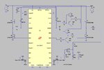
Its the file of the modified schematic that comes with LTspice .

I want to know with maximum power that can be reach with Synchronous buck?
Maximum current at 1 volts output is about 7 ampere.
I prefer to complete the schematic and improve the fault in the design. I have attached the ltspice schematic for better helping. If you run the simulation you can see that the output voltage is reach to 6 volts and after some time it drops to zero because of current limiting. Can you help me for improving my schematic?

Regards
 

Attachments

  • ltc3858-1.jpg
    ltc3858-1.jpg
    141.5 KB · Views: 207

Using a multiphase converter is a good approach for such high currents, so you should use the two outputs of the LTC3858-1 in parallel (with one being slaved to the other). But even so it's probably not suitable for 50A out. The only way it could work is if you use some better external gate drivers. Discrete push pull drivers won't cut it, use something with rail-rail output, and higher drive voltage as well. With only two phases you'll need super size inductors as well...

Anyways your best bet is to use a different controller with four phases and one control loop.
 

Hi,

your external drivers make the signal slower instead of faster and the drive voltages will be less.

The internal gate drive signals are specified with 2.5 Ohms.
You use 10 Ohms in series with the BJTs (they have impedance, too) and additionally your gate drive circuit suffers from dropout voltage to gate_VCC and GND.

Klaus


Hi,

Which chip do you prefer for drivers?
Why do you think you need external drivers?

I recommend to calculate the specifications oir your external drivers... then look for one that fits your needs.
Just connecting something is not a good idea in my eyes.

This IC is not designed for the use of external drivers, maybe look for a better suited IC, as already recommended.

Klaus
 
  • Like
Reactions: tictac

    tictac

    Points: 2
    Helpful Answer Positive Rating
Why do you think you need external drivers?

The transition between the two gate voltage levels requires a certain amount of power to be dissipated in the loop between gate driver, gate resistors and power device.
The gate drivers has to be chosen according to the drive power required for a given power module.
The drive power is calculated from the gate charge Qg , the switching frequency and the actual driver output voltage swing .
I think the LTC3858 gate driver cant supply the current for switching power mosfet.

Qg=90 nc
td(on)=18 ns
tr=10 ns
Peak current for gate=90/28=3.21 Ampere
As you see the current is about 3.2 ampere and this IC cant support this current.

This IC is not designed for the use of external drivers, maybe look for a better suited IC, as already recommended.
Could you suggest better IC ,can uses external drivers ,please ?
 

Hi,

As you see the current is about 3.2 ampere and this IC cant support this current.
True.
But did you do the same calcuation for your driver?
You supply the bootstrap circuit with INTVCC which is 5V.
With max. gate drive voltage (into base of your emitter folowers) of these 5V and the voltage drop in the bjts, the output voltage of your dirvers will be 4V max.
Now with your 10 Ohms resistor.. the current is limited to 0.4A peak (in times when the gate voltage is zero)

This is for sure less than the internal driver can supply.

and besides the decreased current ... it will add additional delay.
and besides this ... it doesn´t care about dead time to avoid cross conduction.
(your driver is symmetric, where the IC internal driver is fast at turn ON (28ns) but even faster at turn OFF (13ns), the difference generates deadtime. essential.)

*****
Could you suggest better IC ,can uses external drivers ,please ?
Not from my mind. I need to go to a manufacturer´s internet site, go to the interactive selection guide, input specifications, get the results.
Read through dtaasheets, read through application notes.

You can do the same.

Klaus
 

You supply the bootstrap circuit with INTVCC which is 5V.
With max. gate drive voltage (into base of your emitter folowers) of these 5V and the voltage drop in the bjts, the output voltage of your dirvers will be 4V max.
If you run LTspice simulation , you can see that the gate-source voltage is about 15 volts.

LTC3858 Gate Driver specification
-----------------------------------------
Tr=25 ns
Cload=3300 pF
-----------------------------------------
So the maximum current is about
I=c*dV/dT
I=3300*10^-12*15/25*10^-9 = 1.98 A

so with this output current from this IC we cant switch IPP08CN10L mosfet as fast as possible . So we need mosfet driver for higher current switching.

Not from my mind. I need to go to a manufacturer´s internet site, go to the interactive selection guide
I think there is not a specific IC that it will be able to provide such a high current and we must design it with mosfet and drivers, Is it true? Would you tell me about the mosfet driver later?
I found LM25117 from Texas that is a Synchronous buck controller with higher output current but one phase driver . What is your idea about it?
 

Hi,

If you run LTspice simulation , you can see that the gate-source voltage is about 15 volts.
I don´t run the simulation.

Datasheet says something different:

BG1, BG2 (Pin 21, Pin 16/Pin 23, Pin 18): High Current
Gate Drives for Bottom (Synchronous) N-Channel
MOSFETs. Voltage swing at these pins is from ground
to INTVCC.


TG1, TG2 (Pin 24, Pin 13/Pin 26, Pin 15): High Current
Gate Drives for Top N-Channel MOSFETs. These are the
outputs of fl oating drivers with a voltage swing equal to
INTVCC – 0.5V
superimposed on the switch node voltage
SW.


INTVCC voltage is specified with typically 5.1V

--> Either the datasheet is wrong your your simualtion is wrong. I assume the simulation, because none of your circuits show a higher supply voltage than 13V... so how can it be 15V?

***************
I think there is not a specific IC that it will be able to provide such a high current and we must design it with mosfet and drivers, Is it true?
The initial question was:
Could you suggest better IC ,can uses external drivers ,please ?
--> If you look for a "better IC": .. (that uses external drivers) ...then this IC usually has no internal high current drivers. It can´t provide high current. This is the job of the external driver.
--> if you look for external drivers: There surey are some with higher current. I don´t do the internet search for you.

Klaus
 

With a few simple changes I was able to get the simulation to work as desired. Here is the file, just change the .txt extension to .asc and run.
View attachment 3858-1_mtwieg1 - Copy.txt

Changes I made from your version:
  1. Slaved output 1 to output 2
  2. Faster soft start (just to make the simulation faster)
  3. Decreased inductors to 1uH
  4. Increased Cout to 1.2mF, decreased its ESR to 5mohm.
  5. Halved the impedance at the Ith pin.
  6. Increased Rsense to 1mohm

Initially your simulation was suffering badly from subharmonic oscillation. Modifications 4-6 help improve this. Especially 4.

This doesn't mean this design is practical. I've built a couple designs in the past where LT controllers showed subharmonic oscillations which weren't predicted by simulation or theory. Your 13V in and 12V out spec might see similar issues. And the power dissipation estimated is definitely a lowball. It estimates efficiency of >95%, I'd expect close to 90%.

The LTC3858-1 doesn't actually say much about the gate drive capabilities. It just states nominal output resistances, but not the peak output current (which is generally less than the drive voltage divided by the drive resistance...). But it may be able to do 2A peak. The actual limitation will likely be thermal inside the controller. Using an external regulator for EXTvcc would certainly help. The application info section in the datasheet discusses this, but doesn't provide any exact guidelines.

I'd still recommend distributing the burden over more phases. The vast majority of LT's multiphase controllers have just two phases, but many have the capability to be slaved to other controllers to make 4, 6, or 12 phase systems. I think a 4 phase converter should be much easier to manage.
 
Last edited:
  • Like
Reactions: tictac

    tictac

    Points: 2
    Helpful Answer Positive Rating
Using a multiphase converter is a good approach for such high currents, so you should use the two outputs of the LTC3858-1 in parallel (with one being slaved to the other). But even so it's probably not suitable for 50A out. The only way it could work is if you use some better external gate drivers. Discrete push pull drivers won't cut it, use something with rail-rail output, and higher drive voltage as well. With only two phases you'll need super size inductors as well...

Anyways your best bet is to use a different controller with four phases and one control loop.

Hi mtwieg
Thanks you for your helps
Would you help me for working on better external gate drivers?

Regards
 

Depends on the FETs you choose to use. UCC27201 or UCC27211 are fairly capable for a wide range of FETs, but will need a supply voltage of at least 8V.
 
  • Like
Reactions: tictac

    tictac

    Points: 2
    Helpful Answer Positive Rating
but will need a supply voltage of at least 8V.
LTC3858-1 can supply voltage higher than 8 volts .
Datasheet says something different:

BG1, BG2 (Pin 21, Pin 16/Pin 23, Pin 18): High Current
Gate Drives for Bottom (Synchronous) N-Channel
MOSFETs. Voltage swing at these pins is from ground
to INTVCC.
But in simulation gate voltage swing from ground to 15 volts. I dont test it really . Do you test it and measuring the voltage range?

Regards,
 

LTC3858-1 can supply voltage higher than 8 volts .
Its internal gate drivers are supplied by an internal regulator fixed at 5.1V. You'll need an external linear regulator to convert Vin into a supply for the external gate drivers.

If the buck's output is higher than 8V then it's possible to bootstrap the gate drivers off of it to save a little bit of power dissipation, but it's probably not worth the effort here.

But in simulation gate voltage swing from ground to 15 volts. I dont test it really . Do you test it and measuring the voltage range?
You're probably just looking at the gate voltage of the upper FET, which will swing from 0V to Vin+5V. But he's referring to the Vgs of each FET, which will only swing by 5V.
 
  • Like
Reactions: tictac

    tictac

    Points: 2
    Helpful Answer Positive Rating
Thanks for reply,

After some searching I found LM25119 that is like LTC3858 but with higher gate current and better specifications. I use Webench designer for designing Synchronous buck with output current at about 50 ampere. but it cant by its regular schematic.
Can I use external mosfet driver for getting higher power for LM25119 ?
lm25119.png
As you see at the picture the Iout(max)=40 ampere. can I design buck with the power of 1kw with this controller?

Regards
 

Attachments

  • lm25119.png
    lm25119.png
    311.9 KB · Views: 162

After some searching I found LM25119 that is like LTC3858 but with higher gate current and better specifications. I use Webench designer for designing Synchronous buck with output current at about 50 ampere. but it cant by its regular schematic.
Can I use external mosfet driver for getting higher power for LM25119 ?
View attachment 145943
As you see at the picture the Iout(max)=40 ampere. can I design buck with the power of 1kw with this controller?
With external drivers, the controller itself shouldn't be a bottleneck. Then the LM25119 and LTC3858 would probably work equivalently.

Again, the smarter way to scale up power is to add more phases, not make each phase bigger.
 
  • Like
Reactions: tictac

    tictac

    Points: 2
    Helpful Answer Positive Rating
Again, the smarter way to scale up power is to add more phases, not make each phase bigger.
You are right. But there is a space limit in my circuit. I dont want to use four inductor and two controller(LM25117) in my circuit . I prefer using two bigger inductor instead of using four smaller one.
So I must using external driver for two phase with LM25119. Would you help me with external driver designing,please?

Regards
 

Status
Not open for further replies.

Similar threads

Part and Inventory Search

Welcome to EDABoard.com

Sponsor

Back
Top