Continue to Site

Welcome to EDAboard.com

Welcome to our site! EDAboard.com is an international Electronics Discussion Forum focused on EDA software, circuits, schematics, books, theory, papers, asic, pld, 8051, DSP, Network, RF, Analog Design, PCB, Service Manuals... and a whole lot more! To participate you need to register. Registration is free. Click here to register now.

My 5v to 7v level shifter, shifts 1.5v to 10v

Status
Not open for further replies.

righteous

Full Member level 2
Joined
Nov 29, 2017
Messages
130
Helped
0
Reputation
0
Reaction score
0
Trophy points
16
Activity points
1,282
Gents,

I made a homebrew level shifter, in the LTSpice simulation it looks ok, but in reality it looks completely different, actually it sucks big time. I wanted it to shift 5v to 7v, but first of all it pulls input down 1.5v and output becomes 10v, even though I only have 7v supply.
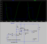
Screenshot from 2018-03-23 18-13-45.png

And this is the scope shot of IN and OUT (of the level shifter)

SDS00001.PNG

Channel 2 (pink) being the digital input.

Any suggestions would be highly appreciated.
 

Congratulations, that circuit is doing exactly what it's supposed. When your input goes high, Q2 turns off. Q4 turns on turning Q1 on. The emitter of Q1 applies about 7V to the gate of M1, turing it off==> 0 volts at Rload.

When the input goes low,Q2 turns on, Q4 turns off and Q4 pulls the gate of M1 to ground==>7 V across the load.

I'm not sure why your scope is showing 10 Volts out, but your simulation looks correct. Your input signal looks a little peculiar for a "digital" signal. And it looks like your output is going BELOW ground. You might have some probing issue.
 

Dear Barry, thank you for your valuable input, unfortunately it does not work. Maybe I expressed myself to vaguely.

The problem is only the "level shifter" i.e. the circuit in the dashed rectangle. It simulates well, and works well when I solder it up; i have a clean 5v digital signal from a MCU entering R5 and a clean-ish 7v square at Q4(e).... until... I connect Q4(e) to the Q1/Q3 pair. Then it becomes like the scope shot, the digital signal from the MCU drops to 1.5v (pink trace 2v/div) and the output (yellow trace) jumps to 10v, and that's the entire problem in a nutshell.

It's not going below ground, if you are thinking of the yellow marker to the right - it's the trigger level indicator.
 

Hi,

I´d say the problem is called "ground bounce".

--> review your GND potential at different places of the circuit. Most probably the high load current (2A) shifts a couple of your "signal_GND" up a bit too much.

I assume "a breadboard circuit"? Or another handmade wiring wihtout taking care of GND currents.

--> show us a photo of your circuit where we can see GND wiring, the pths for the GND currents and the scope connections.

Klaus
 

Dear KlausST

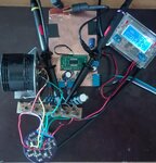
Please see attached photo. I wan't to put the level shift on the driver-PCB in the next iteration, if i can make it work.
Screenshot from 2018-03-24 12-11-56.jpg
 

Hi,

--> show us a photo of your circuit where we can see GND wiring, the pths for the GND currents and the scope connections.

Klaus
 

Yes? I already showed (arrows) where the scope probes are connected, (IN) and (OUT) as per schematic. But I don't understand what you mean by "see GND wiring, the pths for the GND currents". On the MCU copper board, GND is on the top layer. On the level shifter board, it's just a wire. On the driver board, it's a separate GND layer (it's a 4 layer board). The 5v and 7v GND are connected together outside the picture.
 

Hi,

to verify a GND-bounce problem one needs to see where the GND currents flow.

* There is no visible connection for the scope_GND
* there is no visible connection between microcontroller_GND and your circuit_GND
* it´s not clear where the high load currents flow

On the MCU copper board, GND is on the top layer. On the level shifter board, it's just a wire. On the driver board, it's a separate GND layer (it's a 4 layer board). The 5v and 7v GND are connected together outside the picture.
If you want useful help you should show us all this.

Klaus
 

Hi,

If you want useful help you should show us all this.

Klaus

Off course I want useful help, I'm just wondering how to show this without doing the job twice, I think I will make a new driver PCB with the level shifters included, because as you indicate, it's probably an issue with the relative high currents.
 

Hi,

I'm not speaking about PCB.
I speak about GND wiring in general.

And if a photo - where we can see the complete wiring - and some information where the scope_GND is connected is too much effort for you..

And if the recommended mesurement of different GND voltages is asking too much....

... Then helping becomes difficult.

Klaus
 

Hi,

... Then helping becomes difficult.

Klaus

Klaus my dear, I was not implying that your request is unreasonable and that I'm too lazy to do it. I really thought you were talking about the pcb and thinking how to show it. And since I'm old and not an engineer, things do take longer time for me and require more effort and planning. You know; you solder a few wires and measure something, and then suddenly the day has passed without you even notice it, I can't afford too many of those days.

But now that I'm clear on what you mean, I'll revert with a new picture.

- - - Updated - - -

Klaus,

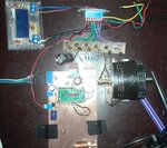
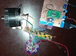
Here's the new picture, this time I added a 4700uF cap on the level shifter board where the supply enters, this 'helped' in the sense that it doesn't draw huge currents and the digital input is not distorted, but the motor obviously won't spin.
IMG_20180325_131814.jpg

And here's the updated scope shot, channel 2 (pink) being the digital input.
SDS00002.PNG
 

Hi,

Again (like in post#4) I rcommend to do somd GND bounce tests.
Now - with the new picture - I can guve mir detailed informations.

* use the scope
* leave the scope_GND at the piece of copper on the microcontroller board.
* connect the tip of the scope to the GND on your level_shifter board.

Now start the program and you will see relatively big voltage difference.
This is the problem.
The microcontroller refers to it's GND ... bug the level shifter refers to another - shifted - GND potential.
This causes malfunction.

The microcontroller output signal (referred to microcontroller_GND) will be good.
But if you measure the same signal at the level_shifter_board (referred to level_shifter_GND) will be too small to operate correctly.

Another thing you should check: is the output voltage of your power supply stable. Does it give enough voltage when the load is switched ON?

Klaus
 

Hi,

I made a sketch about your wiring.
I've arranged the parts according your photo.
Let's focus on the wire from the power supply.

You need thick and short wires from power supply to the round power PCB. (Red, black)
Important: then use short wires from the power PCB --> to the level shifter (red, black)
Then use short wires from level shifter PCB --> microcontroller PCB. (Red, black)

Memo230118_2(2).jpg

Show a photo of your new wiring.

Klaus
 

You can do something else, in addition to what Klaus has mentioned:

completely disconnect you high current motor load, and check the waveforms again.
 

Another thing you should check: is the output voltage of your power supply stable. Does it give enough voltage when the load is switched ON?
Klaus

Check, it's fine as long as the current does not exceed 2.5A - The motor, when it is spinning without the level shifters, is drawing about 400mA

I made a sketch about your wiring.
Klaus

Thank you, please see this photo
IMG_20180327_113052.jpg

I can not power it on for longer than a few seconds, because the level shifters are messing up the signals and shorting the driver FET's i.e. turning on hi and low side at the same time.
 

Hi,

The wiring looks much better now.

I can not power it on for longer than a few seconds, because the level shifters are messing up the signals and shorting the driver FET's i.e. turning on hi and low side at the same time.

So is this a new problem or the same old problem?
You never mentioned HIGH side and LOW side drivers before ... and that they are activated at the same time...

Klaus
 

Hi,

The wiring looks much better now.


So is this a new problem or the same old problem?
You never mentioned HIGH side and LOW side drivers before ... and that they are activated at the same time...

Klaus

Thank you. The hi and low side drivers works perfectly when there is no level shifters, and the motor spins around happily. However when I attach the level shifters the timing (or lack thereof) is turning on hi and low side at the same time, making a short circuit. Hence my conclusion is/was that the level shifters are messing up the signal, the short circuit is therefore just a derived negative effect.
 

Hi,

The hi and low side drivers works perfectly when there is no level shifters, and the motor spins around happily.
I´m confused.
If all worked "perfectly" before, why did you add the level shifters?

From post#1 I assumed you talk about a signal level problem.
Now I'm not sure if there ever was a level problem.
If there was a level problem: is it solved now?

I recommend to solve one problem first before you focus on the next problem.

Klaus
 

Hi,


I´m confused.
If all worked "perfectly" before, why did you add the level shifters?

From post#1 I assumed you talk about a signal level problem.
Now I'm not sure if there ever was a level problem.
If there was a level problem: is it solved now?

I recommend to solve one problem first before you focus on the next problem.

Klaus

I still maintain it's a "signal problem", the FET short circuit only occurs when I add the level shifters.

The reason I added the level shifter is as follows: A desire to increase motor supply voltage which is currently 5v and that works i.e. "works" as in "it's spinning around" -> now I want faster "spinning around" -> So I need to increase motor voltage -> Therefore I also need to add level shifters because the FET's can't be then controlled with 5v logic signals.
 

Q1, Q3 and M1 (referring to schematic) are on the purple round board, I assume, but there are too many SOT packages for your schematic (which I guess would have 6 FETs) and no TO packages for the push pull stage. Can you tell what exactly is in the mentioned board?

The hi and low side drivers works perfectly
So you are actually using driver ICs ? Not the discrete one in post #1 ?

I can not see any decoupling in the power board (i.e. purple round board).

the FET short circuit only occurs when I add the level shifters.
The "OUT" signal is above the threshold of the FETs, so yes, you will have shoot-through if there are FETs in half bridge config.

Can you clarify your actual schematic ?
 

Status
Not open for further replies.

Part and Inventory Search

Welcome to EDABoard.com

Sponsor

Back
Top