Continue to Site

Welcome to EDAboard.com

Welcome to our site! EDAboard.com is an international Electronics Discussion Forum focused on EDA software, circuits, schematics, books, theory, papers, asic, pld, 8051, DSP, Network, RF, Analog Design, PCB, Service Manuals... and a whole lot more! To participate you need to register. Registration is free. Click here to register now.

Tuning rang of cross-coupled delay cell

Status
Not open for further replies.

diego.fan

Member level 3
Joined
Aug 31, 2015
Messages
56
Helped
0
Reputation
0
Reaction score
0
Trophy points
6
Activity points
532
1.png
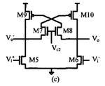
In this paper, there are two sentences:
1. The maximum voltage observed at the gate of M9 is Vg(max)=Vc2-Vtn,. As Vc2 increases the average, gate voltage of the PMOS transistors increases.

2. Large M6 and M10 increases the Vg(max) of M9 and MI0 and hence extends the tuning range.

I'm confused by these two sentences. Which one decides Vg(max) of M9?
 

Re: Tuning range of cross-coupled delay cell

View attachment 145490
I'm confused by these two sentences. Which one decides Vg(max) of M9?

Both, as I understand:

2. Large M6 and M10 (i.e. large aspect (W/L) ratio of M6:M5 and of M10:M9), i.e. by design, and so by a fixed value
and
1. increasing Vc2 by control, i.e. by a variable value
 
Last edited:

Status
Not open for further replies.

Similar threads

Part and Inventory Search

Welcome to EDABoard.com

Sponsor

Back
Top