Continue to Site

Welcome to EDAboard.com

Welcome to our site! EDAboard.com is an international Electronics Discussion Forum focused on EDA software, circuits, schematics, books, theory, papers, asic, pld, 8051, DSP, Network, RF, Analog Design, PCB, Service Manuals... and a whole lot more! To participate you need to register. Registration is free. Click here to register now.

[SOLVED] [Moved]: OTA-C balanced cascode IC design

Status
Not open for further replies.

sherif96

Member level 4
Joined
Feb 22, 2018
Messages
77
Helped
0
Reputation
0
Reaction score
0
Trophy points
6
Activity points
732
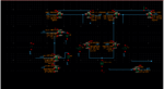
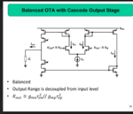
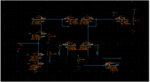
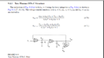
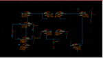
I am designing a balanced ota with cascode output stage attached is my ota schemaitc, however I am still new to IC designing I did not get the hang of the basics yet, such as transistors dimensions and current scaling, I am trying to bias all the transistors in the circuit however the top left and top bottom are always in triode region, I am using a Vdd of 1.2 maximum, what transistors dimensions and V for the two cascodes should I use in such circuit to bias the whole circuit ?
 

Attachments

  • OTA-C.PNG
    OTA-C.PNG
    34.6 KB · Views: 183
  • IMG_20180312_093911.png
    IMG_20180312_093911.png
    100.7 KB · Views: 181

Increase V4 voltage at least 160mV, decrease V2 voltage at least 500mV. Use bigger W/L for top PMOS devices, first double them for example. Those have too high Vdsat.
 
Increase V4 voltage at least 160mV, decrease V2 voltage at least 500mV. Use bigger W/L for top PMOS devices, first double them for example. Those have too high Vdsat.

i am using L value =1u for and width of 4u for both NMOS and PMOS transistors, should I increase the ratio for PMOS or just decrease the ratio for the NMOS ones ?
 

I wouldn't decrease NMOS W/L. But increase PMOS, 4 times maybe. You should go below 200mV Vdsat for all devices. That is normal.
 
I wouldn't decrease NMOS W/L. But increase PMOS, 4 times maybe. You should go below 200mV Vdsat for all devices. That is normal.

I've reached 36u for the widths of the PMOS but still the vdsat is 300+, and for the bottom NMOS all are 400+ how can I fix them to be under 200 ?
 

Attachments

  • Simulation.PNG
    Simulation.PNG
    36 KB · Views: 186

Next time please annotate the node voltages too. I didn't see your circuit is toggled. Without feedback or control voltage you can't ensure to keep the transistors in saturation, because your circuit has got an asymmetric second stage and possibly a hugh gain. It is totally normal that the output voltage is almost equals with the supply rail's voltage then.
Connect NM0's gate to the output and connect NM3's gate to 0.6V. It creates negative feedback, and you can test your circuit with a normal bias condition and set the 2nd stage's transistors.

I thought the voltage was actually annotated as I keep opening and closing cadence the component display parameters change, however I cannot implement what you're asking me to do in the current schematic as I am implementing 3 cascaded stages of the circuit attached, so your advice will be implemented but in the last ota in my design i am still trying to design the general circuit for the rest of the otas, however i still can't bias the circuit, I am using a length of 120n for PM4 and PM2 and a width of 44u, 1u length for PM0 and PM1 and i've tried all width ranges for now I guess but the one in the screenshot would be 100u. I have no idea how to bias the circuit I've tried different currents, different dimension scales but I guess I still do not get all the rules of IC designing and I am still learning
 

Attachments

  • Thomas.PNG
    Thomas.PNG
    46.6 KB · Views: 174
  • Simulation2.PNG
    Simulation2.PNG
    36.3 KB · Views: 176

I don't understand why you cannot implement the feedback for only one stage. To set the proper bias for one stage you should try that. If you set it should be good for more stages.
 
I don't understand why you cannot implement the feedback for only one stage. To set the proper bias for one stage you should try that. If you set it should be good for more stages.

well as far as I understand if I added a negative feedback to my circuit I would be changing the functionality of the circuit itself, arent I ?
 

You should just use the negative feedback until you set the bias conditions. After the operating points are ok, you can break the feedback loop and build the whole 3 stage circuit.
That also use negative feedback to set the transistors into the same operating point what you expect from 1 stage. By the way your 3rd stage is totally connected as I suggested.
I just repeat myself, without feedback you cannot set the operating point of your OTA's 2nd stage because it is assymmetric.
 

Well ok i have connected the negative feedback as you said, but for the first 2 otas in the architecture the first one's feedback is not connected from its own output wont the operating point differ then? And what about the second ota which has no feedback how will i set the bias conditions for this one
 

I don't know the DC values of Vi1, Vi2 and Vi3. Without these I cannot say a good solution. What are the DC values of these sources?
How much are the Gm1, Gm2, Gm3? Also can be important, and a side question, why do you need 3 inputs?
 

I don't know the DC values of Vi1, Vi2 and Vi3. Without these I cannot say a good solution. What are the DC values of these sources?
How much are the Gm1, Gm2, Gm3? Also can be important, and a side question, why do you need 3 inputs?

Nah I do not need the 3 inputs, the architecture supports different transfer functions for different respones, Vi1 and Vi3 are grounded I am only using Vi2 which would be my input signal as Iam building a bandpass filter for which response for the ideal circuit is attached with its ideal circuit schematic, what I need to do next was to replace each vccs with the non ideal circuit of the ota which in our case now the balanced ota with cascode output, I have 3 cascaded stages of the circuit in the previous post each consisting of 3 OTAs, values of gm for the first stage would be: gm1=4.7087u, gm2=6.2282u, gm3=6.2882u, however the next 2 stages do not have equal values for gm 2 and gm3 just the first stage.
 

Attachments

  • FIlter (2).png
    FIlter (2).png
    62 KB · Views: 161
  • BP_Filter.PNG
    BP_Filter.PNG
    17.3 KB · Views: 181

Good, then I assume the Vi1 and Vi3 will be connected to the common mode voltage which should be the half of the supply voltage, for optimal output swing.
In this case the DC voltage in your circuit at every output and input nodes of the Gm cells should be around 0.6V. This ensures that every stage use the same biasing condition and you can use the same method what I suggested for you for every Gm stage to set the proper operating points.
You can set all stage separately then connect them and it will be good.
 

Last question how can i use the feedback method you suggested for the first and second ota where they do not have a negative feedback?
 

Connect NM0's gate to the output and connect NM3's gate to 0.6V. Repeat this for every stage separately, set the desired Gm and proper operating points for the transistors then break this feedback and connect the separately designed stages together by your figure from that book.
 

Just to make sure i understand correctly, you want me to remove v1 and v3 , instead of v1 i add a dc voltage of 0.6, instead of v3 i connect a negative feedback to the output and then set the operating point and my gm values correct?
 

No. I said set the operating points separately. When the stages are not connected together, connect NM0's gate to the output and connect NM3's gate to 0.6V. Set Gm and Vdsat.

After you finished connect the stages together by your figure and connect Vi1 and Vi3 to 0.6V common mode voltage.
 

No. I said set the operating points separately. When the stages are not connected together, connect NM0's gate to the output and connect NM3's gate to 0.6V. Set Gm and Vdsat.

After you finished connect the stages together by your figure and connect Vi1 and Vi3 to 0.6V common mode voltage.

It should look something like this am I right?Simulation Feedback.PNG
 

V5 should be removed. Presently the amplifier output is shorted.
 

Status
Not open for further replies.

Similar threads

Part and Inventory Search

Welcome to EDABoard.com

Sponsor

Back
Top