sherif96
Member level 4
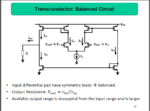
V5 should be removed. Presently the amplifier output is shorted.
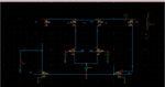
however if I removed v5, when I remove the feedback wire after setting the dc operating points and my gm value wouldnt the circuit be incomplete as the differential pair are not identical ?
- - - Updated - - -

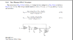
a question concerning the gm value, if the value of gm is increasing through my bandwidth as follows, how can I make it constant over my required bandwidth ?