Continue to Site

Welcome to EDAboard.com

Welcome to our site! EDAboard.com is an international Electronics Discussion Forum focused on EDA software, circuits, schematics, books, theory, papers, asic, pld, 8051, DSP, Network, RF, Analog Design, PCB, Service Manuals... and a whole lot more! To participate you need to register. Registration is free. Click here to register now.

NMOS Devices with different Bulk Potentials

Status
Not open for further replies.

bwarlord01

Junior Member level 3
Joined
Sep 2, 2017
Messages
25
Helped
0
Reputation
0
Reaction score
0
Trophy points
1
Activity points
194
Hi guys, i just wanna ask, what layers should i add in my NMOS Layout in order to prevent short circuit from other NMOS Devices, since these NMOS Devices have different bulk potentials.

I am using TSMC 65nm CMOS Process Technology.

I am a bit confused about these NWELL, PWELL, DNWELL, and i dont know what to do to make my layout work
 

I am not familiar with your process but you may be able to put them into different pwells or dnwells.
 

Capture.JPG
as you can see in the attached photo, my 2 nmos are having different bulk potentials. idk how to fix this problem in my layout, it says that it is shorted, i have already added an outer layer PWELL and NWELL in both NMOS transistors.
 

Do your nmos devices sit inside separate nwells?
 

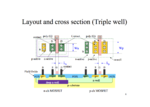
You need two different nwells with one PMOS and one NMOS (in its pwell in the same nwell) each for the two upper and the two lower MOSFETs of your above schematic. Here's an image of one of these two nwells:
Analog_layout_design_Kanazawa_University_p6.png
Both Bulk and both Source contacts are connected with each other (all 4 are at the same node).

Note: the DNW (deep nwell) isn't absolutely necessary; a common nwell is sufficient.
 

Status
Not open for further replies.

Part and Inventory Search

Welcome to EDABoard.com

Sponsor

Back
Top