Continue to Site

Welcome to EDAboard.com

Welcome to our site! EDAboard.com is an international Electronics Discussion Forum focused on EDA software, circuits, schematics, books, theory, papers, asic, pld, 8051, DSP, Network, RF, Analog Design, PCB, Service Manuals... and a whole lot more! To participate you need to register. Registration is free. Click here to register now.

What knife do you use for cutting copper for microstrip?

Status
Not open for further replies.

skatefast08

Full Member level 3
Joined
Jan 24, 2018
Messages
189
Helped
2
Reputation
4
Reaction score
2
Trophy points
18
Activity points
1,779
What specific type of knife is best used for cutting copper for microstrip? and what website could I get this product?
thanks
 

Microstrip is created by etching a PCB. What do you mean about "cutting copper" with a knife?????
 

Hi,

If you mean cutting into a copper clad board, for hobby or prototype stuff, which no doubt you don't, but anyway, I find a cutter (/exacto knife I think it's called in the USA) is a good choice. New blades dig into the copper/board and can stick; once a blade segment is old/used a fair bit, the cuts between tracks become sloppier and marginally wider due to the lack of sharpness and precision. It is uncomfortable after a couple of hours if it is rectangular. You could use any strong enough arts and crafts scalpel-style knives as well, and that might be more comfortable to hold for long periods, especially those with plastic handles/stems.

If you expect to cut a microstrip by hand, the inaccuracies are going to be so great that you shouldn't even bother. There's no way you're going to be able to cut, say, a 14 mil trace.
 

https://www.eeweb.com/tools/microstrip-impedance using this calculator, I am using an FR4 board: H = 1.5mm, T = 0.05mm, W = 2.7mm, and Er = 4.7.... So, I want to cut the coppers width at about 2.7mm in width (not 14 mil). I am trying to design my own 2.4 GHz LNA with this, on https://www.farnell.com/datasheets/1644697.pdf it says Er = 4.7 at 1 GHz, but Im guessing Er isn't going to be much of a significance since I am working at 2.4 GHz?

- - - Updated - - -

https://www.eeweb.com/tools/microstrip-impedance using this calculator, I am using an FR4 board: H = 1.5mm, T = 0.05mm, W = 2.7mm, and Er = 4.7.... So, I want to cut the coppers width at about 2.7mm using adhesive copper tape.
 
Last edited:

I have never had any luck cutting "soft" substrates, such are rogers duroid. The dielectric material is so soft that the knife dents into it more than cutting.

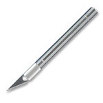
FR4 boards, being very stiff, can easily be cut. I use an Exacto knife with a stout handle and the big blade.
knife.jpg

I cut the area i do not want copper on, then use a soldering iron tip set at very hot to heat up the copper, and it peals away easily. Put the board on a non slip surface so it does not move....i just use my antistatic rubber mat top on the workbench.

Watch your fingers, as you have to put a lot of force on the knife.

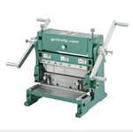
To cut FR4 board for prototyping, i use a sheet metal shear:
shear.JPG
it is also handy for cutting copper sheet, for forming horns, antennas, emi shields, etc.

- - - Updated - - -

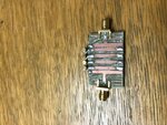
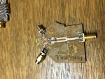
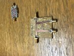
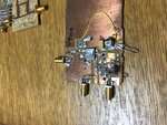
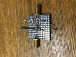
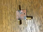
it is going to be a crude circuit, but often that is all you need to do a simple circuit function during a prototype system test. Some random circuits i had lying around:
IMG_2745.JPGIMG_2746.JPGIMG_2747.JPGIMG_2748.JPGIMG_2751.JPGIMG_2752.JPG

Note the one with the pre-printed protoboard squares...i use those a LOT for circuits that have plastic packed SMT devices, like amplifiers.

you can get protoboards here:
https://www.busboard.com/SP2-100x100-G

they have 100 x 100 mil pads (the ones i use) or 50 x 50 mil pads
 
Last edited:
For cutting traces in an existing PCB do I also use an exacto but with a blade where I have intentionally broken the tip at a sharp angle. That makes it possible to create traces using knife as a chisel and avoids creating a trench in CU layer as it else easily becomes with a knife.
If prototyping a complete board do I remove all copper at top layer and creates new traces with CU-tape which is easy to cut with a scissor to needed width before applied at PCB.
It is then also easy to increase trace width by replacing whole trace with a new strip CU-tape.
 

F
If prototyping a complete board do I remove all copper at top layer .
I am assuming you mean "all unused copper at the top layer". Normally it does not matter if you leave unused metal on the top.
But i have seen cases where that extra metal forms a parallel plate resonator with the ground plane underneath, and causes havoc. In those cases, you drill a hole thru the board in a few places, and run a copper wire from top to back, and solder it to both sides. that will "short out" the resonator, and keep things happy.

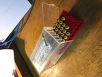
BTW, when you try to drill small holes in a PC board, EXPECT the drill to break. So WEAR SAFETY GLASSES, and have lots of standby drills. I buy big boxes of re-sharpened carbide drills the PC board houses use and throw away, just for this purpose.

drill.JPG

These are 0.035" diameter
 
  • Like
Reactions: d123

    d123

    Points: 2
    Helpful Answer Positive Rating
Status
Not open for further replies.

Part and Inventory Search

Welcome to EDABoard.com

Sponsor

Back
Top