Continue to Site

Welcome to EDAboard.com

Welcome to our site! EDAboard.com is an international Electronics Discussion Forum focused on EDA software, circuits, schematics, books, theory, papers, asic, pld, 8051, DSP, Network, RF, Analog Design, PCB, Service Manuals... and a whole lot more! To participate you need to register. Registration is free. Click here to register now.

[SOLVED] Gate driver problem, Optocoupler is destroyed everytime

Status
Not open for further replies.

shomikc

Member level 4
Joined
Apr 19, 2013
Messages
71
Helped
0
Reputation
0
Reaction score
0
Trophy points
1,286
Activity points
1,951
Hello all,

I am using the following Gate Driver for IRF 640 MOSFET.

My Optocoupler TLP 250 keeps getting destroyed.
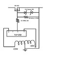
gate drive circuit.jpg

I don't know what I am doing wrong but it seems that high current is being drawn.

The transformer supplies power top the optocoupler through voltage regulators 7815 and 7915.

Any help on shedding a little light on my problem will be much appreciated.

Thanks.
 

Hi,

your schematic is misleading...with the transformer connected directly to the TLP250. Thi
Your text says something different. This is confusing.
Additinally I don´t see any power supply cpacitors...and we don´t see the driving circuit for the TLP250
--> Please post your "true schematic".

Give informations like switching frequency, duty cycle...

While driving a FET´s gate with +/-15 is not wrong ... but it is very unusual.
There are lot´s of schematics in the internet how to drive a MOSFET with a photocoupler.

Klaus
 
The transformer supplies power top the optocoupler through voltage regulators 7815 and 7915.
That's more than the posted schematic shows, but there should be also a rectifiers and filter capacitors. Asking too much to expect a complete schematic?

My Optocoupler TLP 250 keeps getting destroyed.
No particular reason suggested by the schematic (if we assume a meaningful power supply, see above).

Sure that the MOSFET is still healthy? Coupler damaged by a shorted MOSFET would be quite plausible.
 
What does the failure signature tell you about likely
mechanisms / causes? For starts, is the emitter or
the phototransistor what's getting damaged, is it
overcurrent or overvoltage (you might need to blow
up some more, with added components, to keep one
from becoming the other so you can see).

Failure analysis is a very useful faculty to cultivate.
Asking "Wha' happen?" to strangers with only the bare
minimum of context is usually much less successful.
 
I’ll echo the chorus that an actual, well drawn schematic would help.
Enormously.

Also an actual description of the failure symptoms, and a description of what you are attempting to drive with the Mosfet.
 
Hi all,

I am sending an almost completely accurate picture of my circuit.

circuit.jpg

I hope this will help.

The switching frequency is 25kHz and the circuit is a voltage mode controlled Buck chopper.

Thanks.
 

No obvious reason why TLP250 should be damaged.

Grounding the power circuit to the switching node seems strange, also sensing the output voltage relative to the switching node by the pwm controller.
 

Hi,

I recommend not to use the -15V for driving the MOSFET. Just connect pin5 of TLP250 to GND. This helps to speed up switch ON timing.

The control_circuit (SG3524) and the gate_driver_output refers to the same GND, thus an isolator is not necesary.

Your issue:
your 12V DC supply doesn´t refer to the GND. Thus the voltage regulation of the output will not work.
In other words: The feedback node R9/R10 does not have the same reference as the control circuit.

The solution is to break the GND connection between Gate_driver_circuit and control circuit. (Then you need the isolating gate driver)
Then connect 12V_GND with control_circuit_GND.

Klaus
 

FvM Sir,

I thought this was the usual practice. Can you please tell me what is normally done in both the situations you have mentioned.

- - - Updated - - -

Klaus Sir,

I have not been able to show it exactly in the diagram, but I have done exactly as you have said. The Gate Driver ground and Control Circuit ground are different and the power circuit return path is connected to the control circuit ground.

Also is it possible to know if my MOSFET has been shorted out as Mr. FvM had pointed out in an earlier post.

Thanks.
 

I have not been able to show it exactly in the diagram
What's the problem with using different ground symbols in the schematic?

Also is it possible to know if my MOSFET has been shorted out
Use a multimeter?
 

Thankyou for your help to everyone. I made mistake by being inaccurate. It will not happen again.
 

Some IGBT drive circuits require a negative bias, Mosfet drive certainly dos not.

To repeat what everyone else has mentioned already: a buck topology is a classic example of a non-isolated topology. This essentially means that all the grounds have to be tied together.
As such, an isolated driver is not necessary.
 

To repeat what everyone else has mentioned already: a buck topology is a classic example of a non-isolated topology. This essentially means that all the grounds have to be tied together.
As such, an isolated driver is not necessary.

This buck topology needs a driver floating with MOSFET source ("switching node"), its power supply can't be tied to DC-. In so far, the OP's explanation in post #9 is plausible, the schematic should be corrected in this regard -> DC- tied to pwm controller GND, gate driver has separate floating GND tied to MOSFET source.
 

Of course, FvM. The Mosfet's source return line is not ground.

What I should have said is that the input and output grounds are common and non-isolated from each other.

However..........The floating high side drive of the Mosfet is achieved with the proper high side driver IC which performs the necessary level shifting.
 

Status
Not open for further replies.

Similar threads

Part and Inventory Search

Welcome to EDABoard.com

Sponsor

Back
Top