- Joined
- Jul 4, 2009
- Messages
- 16,235
- Helped
- 5,140
- Reputation
- 10,309
- Reaction score
- 5,120
- Trophy points
- 1,393
- Location
- Aberdyfi, West Wales, UK
- Activity points
- 137,396
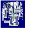
Much better!
Are you sure the PC817 can handle the relay coil current? I think transistor drivers would work better.
Personally I would make these changes:
1. move the track from F2 to the relays to a position more central between the relay pins and make it wider.
2. where C1 and C2 are linked, remove the track to ground and wire a new track from them directly to the MCU.
3. Flood fill the grounds wherever possible.
Brian.