Continue to Site

Welcome to EDAboard.com

Welcome to our site! EDAboard.com is an international Electronics Discussion Forum focused on EDA software, circuits, schematics, books, theory, papers, asic, pld, 8051, DSP, Network, RF, Analog Design, PCB, Service Manuals... and a whole lot more! To participate you need to register. Registration is free. Click here to register now.

Too much vias in layout? What are the consequences?

Status
Not open for further replies.

AllenD

Member level 5
Joined
Aug 7, 2017
Messages
91
Helped
0
Reputation
0
Reaction score
0
Trophy points
6
Activity points
1,193
Too much vias in layout? Whats the consequences?

Hi My friends,

In an IC layout, is there such thing as too many vias?
I am using TSMC 65 nm CMOS to layout some circuit. My methods to place vias is "as much as possible" so that the resistance will be smaller. As the result, there are a LOT of vias in the layout. However, an experenced designer in my lab told me he would not place so much vias. He could not conclusively know what will be the consequences expect potential metal density failure.

Can anyone help me? If there are too many vias, what could go wrong?

Thanks
Allen
 

Re: Too much vias in layout? Whats the consequences?

I don't think "too many bias" should be a concern - unless you violate some design rules (e.g. vias too close to each other) - in which case you will see DRC violations.
 

Re: Too much vias in layout? Whats the consequences?

If there are too many vias, what could go wrong?

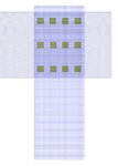
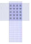
If you use a dense via array (min. spacing) at a branch connection from a current-leading wide supply rail, you'd better omit every second via row in current direction in order not to disturb/narrow the current flow too much.
 

Re: Too much vias in layout? Whats the consequences?

If you use a dense via array (min. spacing) at a branch connection from a current-leading wide supply rail, you'd better omit every second via row in current direction in order not to disturb/narrow the current flow too much.

Erikl - I don't understand the physics of the effect you are referring to (maybe a simple drawing can help understand it), and never heard of this technique used in IC layouts - can you elaborate?
 

Re: Too much vias in layout? Whats the consequences?

This depends on the vias and the next layer of metal.

I have worked in hot-dep aluminum technologies where
(say) Met2 is the source for Via1 fill. Works well when it
works well. When it does not, the vias draw too much
material from the flat field and you get sidewalls that are
too thin or even voided.

This drove special large-bed via rules (>2x2 arrays) that
require more spacing, so as to enforce more accessible
fill-volume and more repeatable filling.

This issue was discovered at FOK fab on a DX federal
program, with predictable levels of joy and camaraderie.
I had to go and ream out every via-bed in the power
grid by hand, cutting quantity by half (fortunately my
layout style is to put as many vias as will fit the bussing
so that I get less density rule knocks).

Tungsten-plug vias as are common in more modern CMP
stacks, don't want anything from the abutting layers.
This has its own electromigration consequences (which
may or may not be properly characterized or expressed
in the layout rules).

In newer technologies you may see max as well as min
layer density rules and furthermore, these may be small-
field / "porthole" (not chip extent) based, if there are
any known lithography issues attending high density
(min density is often more about auto-align goings-on,
at least for negative features; positive features also may
have over-etch concerns). Sometimes "lonely vias" are
also probe to overetch, or a process tuned for the
"lonely" via may then underetch in large beds or high
density routing.

CMP interconnect doesn't suffer the current-flow
disturbance / crowding as much as non-planarized (non-
plug) via fills, there is no sidewall "choke point".
 

Re: Too much vias in layout? Whats the consequences?

Theoretically, all that deep technology knowledge should be encapsulated in design rules, and the designer should be abstracted from it.
You create the layout, and DRC/LVS should tell if that's good or not.
 

Re: Too much vias in layout? Whats the consequences?

If you pass the design rules then you should be OK. Pay attention to any matched routes and high current paths. Matched routed should have the same number of vias. Current crowding is the concern with high current paths and may require some customization of vias.
 

Re: Too much vias in layout? Whats the consequences?

Erikl - I don't understand the physics of the effect you are referring to (maybe a simple drawing can help understand it), and never heard of this technique used in IC layouts - can you elaborate?

Hi Max,
instead of this: via-array_0.jpg

... I used to leave out every second row in main current flow direction: via-array_1.jpg

This had been recommended by experienced reliability people in order not to narrow the current flow in the main rail too much. Perhaps you could simulate such a phenomenon?

I used to do this in 0.35 down to 0.13µm processes, before and after CMP planarization was in use.
 

Re: Too much vias in layout? Whats the consequences?

erikl -

In my view, both resistance and current density in vias will be higher in the second case.
I do not see how every other via row removal can help with anything here.
The effect can be easily simulated, with the right tool.

Max
 

Re: Too much vias in layout? Whats the consequences?

In my view, both resistance and current density in vias will be higher in the second case.

Sure, Max,

but that's not the problem if you still have enough vias. The reliability guys' concern was the current crowding by the vias in the main supply rail, and the interrelated (possible) reliability problem due to therein increased electromigration.

erikl

PS: May be there's a misunderstanding due to the drawings above: the horizontal rail doesn't end at the right side, it's just a section of a long supply rail.
 
Last edited:

Re: Too much vias in layout? Whats the consequences?

Too much vias will increase the stress immunity of the die.Not too less nor too much.
 

Re: Too many vias in layout? Whats the consequences?

Too much vias will increase the stress immunity of the die.

But wouldn't increasing the stress immunity of the die be a rather positive result:?: :grin:
 

Re: Too many vias in layout? Whats the consequences?

But wouldn't increasing the stress immunity of the die be a rather positive result:?: :grin:
Yes, the phrase is not correct.I meant the die will be more sensitive to stress.:thumbsup:
 

Re: Too much vias in layout? Whats the consequences?

I have never seen a stress related / based rule for via
density.

I would be interested to see anything about the
mechanics or any impact to devices' electricals.
 

Status
Not open for further replies.

Part and Inventory Search

Welcome to EDABoard.com

Sponsor

Back
Top