Continue to Site

Welcome to EDAboard.com

Welcome to our site! EDAboard.com is an international Electronics Discussion Forum focused on EDA software, circuits, schematics, books, theory, papers, asic, pld, 8051, DSP, Network, RF, Analog Design, PCB, Service Manuals... and a whole lot more! To participate you need to register. Registration is free. Click here to register now.

Common mode noise issue in offline LED driver (150W)

Status
Not open for further replies.
T

treez

Guest
Hello,
Please assist us in solving our Common mode noise problem?

We have designed an Offline 240VAC LED driver which is linear regulator based. (86% efficient).
It does however contain a 1W Buck converter for its bias supply.
The schematic of the salient parts, and the filter components, is as attached in the pdf.

For cost reasons, we are not allowing ourselves to use any through hole components on the PCB. We are also not allowed any custom made components (only offtheshelf allowed). We are also not allowed to take an earth wire connection to the PCB, as its more cost due to the greater assembly effort. (the Earth wire does, however, connect to the earthed heatsink on which the PCB sits, and is held onto by metal screws)

For the following Conducted EMC scans, we changed the values of some of the filter components shown in the pdf…….changing the Inductor values to try and get it to pass conducted EMC….

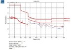
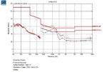
We started off with scan A. The filter values for this were as in the schematic.
Scan A is a fail around 150Khz.
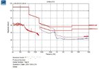
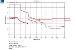
Therefore we changed the damping resistors (R2,R3) to 1k, as in scan B, and then it was still a fail at 150kHz, but less badly failing than A.
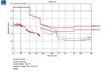
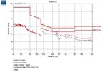
Therefore we kept the 1k resistors for R2 and R3, and then increased L3 from 47uH to 100uH as in Scan C. However, this was worse than scan B at the failure frequency of 150kHz. That is, increasing the filter inductance, made the conducted scan worse. This made us realise that our problem is predominantly a common mode problem. 150kHz is not a usual frequency for a common mode problem, but as you know, the 150kHz is simply the frequency of the” envelope” which comprises the much higher frequency common mode disturbances.
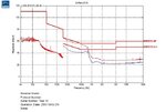
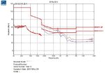
Anyway…we then reduced L3 to 22uH and finally got it to pass (hoorah!) as in scan D.
However, the readout for scan D strangely says it’s a fail at 150kHz because it recorded exactly 66dBuV and that is exactly what the limit line is at. –So the official readout said that we failed by zero dBuV (!!!).

Anyway, in a desperation to get further below the limit line, we then kept L3=22uH, and kept R2,R3=1k, but increased L4 and L5 each from 100uH to 150uH. This is shown in scan E.
..However, this is worse than scan D. –It fails badly around 500kHz. Again it showed that increasing the filter inductance, made the results worse.
However, decreasing L4 and L5 each from 100uH down to 47uH also made the result worse. So therefore we have currently stuck with R2 & R3=1k, L3=22uH, L4 & L5 = 100uH. (ie scan D) The rest is as in the schematic shown.

However, as scan D shows, we are too close to the limit line, and need to reduce the noise more….

Buck switching node:

We believe that much of the problem common mode noise, is emitting from the switching node of the 1W Buck converter. (we know this from previously reducing the switching node copper size and taking EMC scans).

Shielding the switching node from the earthed heatsink:
For the above scans (A-F), we also shielded the Buck’s switching node copper from the Earthed Heatsink by laying copper pours in the internal and bottom PCB layers below the switching node copper. The shielding layers are connected to circuit ground. –We are now wondering if this is a mistake? In fact, we wonder if we should have used the 13V rail net for the shielding layers? The problem with using circuit ground as the shielding layers , is that there is a large circuit ground copper pour over most of the bottom layer of the PCB, which lies on the earthed heatsink. As such, we fear that having circuit ground as our shield for our switching node, is actually in some way injecting too much switching node noise into the earthed heatsink and exacerbating our common mode noise problem? Should we instead use the 13V rail net as our shielding layer? (to go between the switching node and the earthed heatsink).

EMC capacitors coupling to Earth ground.
As discussed, we don’t have an earth wire connection to the PCB. However, the PCB is held onto the earthed heatsink by metal screws. We are thereby wondering if we can thereby do the following so as to further decrease our common mode noise problem?......We could plate under the head of one of the screws with bare PCB copper. In this way, we would get some PCB copper which was directly connected to Earth ground. We could then couple the 13V rail net (ie a ‘quiet’ node) to this Earthed copper by using a 100pF capacitor. (4kV,2225,X7R)
Do you think that this would help decrease our common mode noise problem?
 

Attachments

  • 150W LED driver.pdf
    15.1 KB · Views: 124
  • A.jpg
    A.jpg
    75.6 KB · Views: 192
  • B.jpg
    B.jpg
    74.9 KB · Views: 186
  • C.jpg
    C.jpg
    74.2 KB · Views: 187
  • D.jpg
    D.jpg
    74 KB · Views: 180
  • E.jpg
    E.jpg
    74.4 KB · Views: 200
  • F.jpg
    F.jpg
    74 KB · Views: 192

How to propose to analyze common mode EMC without including earth in your schematic? Do you not have any Y capacitors? Do you have an estimate of the capacitance between GND and earth?
 
  • Like
Reactions: treez

    T

    Points: 2
    Helpful Answer Positive Rating
How to propose to analyze common mode EMC without including earth in your schematic? Do you not have any Y capacitors? Do you have an estimate of the capacitance between GND and earth?
Thanks, the Earth wire from the mains is connected to the heatsink. (not to the PCB). The PCB lies on the earthed heatsink (on top of the thermal pad). As you infer, the capacitance to Earth is just the stray capacitance of the PCB/heatsink interface, and the stray capacitance of the LEDs to the (same) earthed heatsink. I am afraid we don’t know how much this is. We have no Y caps (other than ‘stray’ ones) and cannot have normal Y caps, because we don’t have Earth on the PCB, and we are not allowed PTH components. We are not allowed an Earth wire to the PCB because it would mean more production assembly effort and cost.

However, I suspect that you are thinking the same as me(?), that indeed we can “kind-of” have Y caps…that is, the metal screws that screw the PCB to the Earthed heatsink could have PCB copper underneath their heads…..and then this PCB copper would be ‘Earthed’ PCB copper (due to its abutting the metal screw which is in the earthed heatsink) ….we could then put some high voltage ceramic capacitance between this Earthed Copper and a ‘quiet’ node on the circuit…..voila…..Y capacitors.
Do you think this would be worth doing?

Another point is that we did another EMC scan (attached) which was with a unit with the LEDs having thicker thermal pads beneath them…..ie, giving less stray capacitance between the LEDs and the earthed heatsink……this gave a worse conducted emissions result than the other unit which had a thinner thermal pad (ie comparing it with scan A above)….so this is pointing to the fact that doing our little trick with screws/Earthed PCB copper/Ceramic caps may work and reduce conducted emissions (because it will increase capacitance to Earth from a 'quiet' circuit node) …do you agree?

Also, what about using the 13V rail net as the shield instead of circuit ground (as discussed in top post)?
 

Attachments

  • With thicker thermal pad below LEDs.jpg
    With thicker thermal pad below LEDs.jpg
    74.7 KB · Views: 208
Last edited by a moderator:

Without Y capacitors you have no way of addressing CM interference except reducing the interference source, or increasing CM impedance of your line filter. Why don't you use an actual CM choke instead of two inductors? CM chokes can be found in SMT packages.

I'm not actually convinced this is purely CM interference at work. As usual, the measurement method isn't explained thoroughly.

Also, what about using the 13V rail net as the shield instead of circuit ground (as discussed in top post)?
I don't see why that would help.
 

Why don't you use an actual CM choke instead of two inductors? CM chokes can be found in SMT packages.
Thanks, All the CM chokes we've found in SMT, are too high in profile.....we need it to be less than 8mm high.

I'm not actually convinced this is purely CM interference at work. As usual, the measurement method isn't explained thoroughly.
Thanks, you're right, the plots show both CM and DM noise. As can be seen from my top description, the fact that increasing the inductances often makes the scans worse shows that its really CM noise that is the biggest problem factor for us.

Also, what about using the 13V rail net as the shield instead of circuit ground (as discussed in top post)?
I don't see why that would help.
Thanks, ..we were thinking, ..because the gnd net is most highly capacitively coupled to the earthed heatsink, and also using it as the shield could mean actually coupling the switching node interferences to the earthed heatsink.....the opposite of what we want. The 13V net is not spread over the bottom layer of the PCB and so is much less capacitively coupled to the heatsink...therefore we wonder if it would be a better sheild for the switching node of the 1W buck.
Basically , we think the shield should be a quiet node, and with as little capacitive coupling as possible to the earthed heatsink, would you agree?

Without Y capacitors you have no way of addressing CM interference except reducing the interference source, or increasing CM impedance of your line filter.
Thanks, as such, would you thereby agree that the little trick with connecting capacitors from circuit gnd to earthed pcb copper which connnects to earth via the metal screws is a good idea? (we cannot take an earth wire connection to the pcb...it would add too much cost/size and assembly effort. -this is very cost sensitive.)

- - - Updated - - -

Regarding the use of the 13V net as a shield instead of circuit gnd, do you think this may actually make CM noise worse on the conducted EMC scans?
 
Last edited by a moderator:

Thanks, you're right, the plots show both CM and DM noise.
No, the two traces show average and QP of the same signal. There's no indication I can see as to what is actually being measured (line, neutral, or some combination of the two).
As can be seen from my top description, the fact that increasing the inductances often makes the scans worse shows that its really CM noise that is the biggest problem factor for us.
Without knowing what is actually being measured, I don't think you can be sure.


Thanks, ..we were thinking, ..because the gnd net is most highly capacitively coupled to the earthed heatsink, and also using it as the shield could mean actually coupling the switching node interferences to the earthed heatsink.....the opposite of what we want. The 13V net is not spread over the bottom layer of the PCB and so is much less capacitively coupled to the heatsink...therefore we wonder if it would be a better sheild for the switching node of the 1W buck.
The 13V rail is connected to GND via some bypass capacitors. If those bypass caps have decently low ESR and ESL, then GND and 13V should effectively be shorted together for high frequencies. If that's the case, interchanging them won't matter at all.

Thanks, as such, would you thereby agree that the little trick with connecting capacitors from circuit gnd to earthed pcb copper which connnects to earth via the metal screws is a good idea?
Using screws to the heatsink could be a fine way to connect earth to your circuit without wiring it to the PCB. But rather than connecting the caps from earth to circuit GND, you should connect them to the line inputs, like proper Y caps (Y caps can be found in SMT packages).
 
  • Like
Reactions: treez

    T

    Points: 2
    Helpful Answer Positive Rating
i think first we need to check if the noise is it common or differential mode, because based on that we can select the right solution, you can check that by connecting a current probe instead of the LISN and then you measure the noise in one line or in both lines, differential mode can be solved by slecting the right filter between the lines, and common mode by using ht eright CM choke, we can help to find CM choke less than 8mm, but we need to have the ratings of your circuit.
 
  • Like
Reactions: treez

    T

    Points: 2
    Helpful Answer Positive Rating
Quote Originally Posted by treez View Post
Thanks, you're right, the plots show both CM and DM noise.
No, the two traces show average and QP of the same signal. There's no indication I can see as to what is actually being measured (line, neutral, or some combination of the two).

Thanks, the scans shown are the neutral scans.( They put a little letter "N" at the end of the number on the top bit of the scan. ) There is a corresponding Live scan for each case, but i didnt bother showing them as they are the same in each case.

Yes i agree they do show QP and average. I am certain its both DM and CM noise. We didnt ask them to use a splitter to separate out the CM and DM disturbances.
we need to have the ratings of your circuit.
Thanks, its 150W, and 240VAC input. Power factor corrected.

Using screws to the heatsink could be a fine way to connect earth to your circuit without wiring it to the PCB. But rather than connecting the caps from earth to circuit GND, you should connect them to the line inputs, like proper Y caps (Y caps can be found in SMT packages).
Thanks, yes I agree we should really connect the Y caps to line inputs. Unfortunately, due to where the screws are, we cannot do this. So I believe we have to do the next best thing, and just connect circuit GND to the earthed copper with high voltage coupling capacitors. (Ceramic SMD). The capacitors will have to go right by the screws. There’s no room to do it any other way.
…..I believe that this will help……surely?....after all, the “stray” Y capacitor provided by the stray capacitance of the LEDS and their mountings to the earthed heatsink created a stray Y capacitor and that helped us with the conducted EMC scans…the attached two EMC conducted scan plots show that the unit with the thinner thermal pads beneath its LEDs performed better with conducted EMC…. This is because it formed a larger stray Y capacitance….that is, the benefit was seen even though these stray Y capacitors don’t go back to the line inputs. Though I agree that what would be best would be proper Y caps connecting from earth to line inputs….but we can’t do it that way. Its one of our constraints unfortunately.

The 13V rail is connected to GND via some bypass capacitors. If those bypass caps have decently low ESR and ESL, then GND and 13V should effectively be shorted together for high frequencies. If that's the case, interchanging them won't matter at all.
Yes i agree, but that slight bit of ESL and ESR might be all thats needed to tip us that tiny bit below the limit line...and give us a pass...rather than our scan D in the top post, which has us failing by what they say is zero dBuV. It was bang on the limit line at 150kHz so they said its a fail.
 

Attachments

  • With thicker thermal pad below LEDs.jpg
    With thicker thermal pad below LEDs.jpg
    74.7 KB · Views: 113
  • With thinner thermal pad beneath LEDs.jpg
    With thinner thermal pad beneath LEDs.jpg
    75.6 KB · Views: 213
Last edited by a moderator:

Thanks, the scans shown are the neutral scans.( They put a little letter "N" at the end of the number on the top bit of the scan. ) There is a corresponding Live scan for each case, but i didnt bother showing them as they are the same in each case.

Yes i agree they do show QP and average. I am certain its both DM and CM noise. We didnt ask them to use a splitter to separate out the CM and DM disturbances.
Data taken only from line or neutral cannot allow you to distinguish between CM and DM signals. If you had kindly asked them to perform a measurement of L+N or L-N then that would have been very useful.

Thanks, yes I agree we should really connect the Y caps to line inputs. Unfortunately, due to where the screws are, we cannot do this. So I believe we have to do the next best thing, and just connect circuit GND to the earthed copper with high voltage coupling capacitors.
I don't think this would help your EMC issues though. In fact I would bet on it making the CM interference worse. A capacitor from earth to GND will allow interference from your SMPS to bypass the line filter entirely on its way to earth. A proper Y capacitor, on the other hand, diverts that interference from your heatsink back to line and neutral, away from the earth wire.
 
  • Like
Reactions: treez

    T

    Points: 2
    Helpful Answer Positive Rating
Data taken only from line or neutral cannot allow you to distinguish between CM and DM signals.
Thanks, yes we agree with that. We've always been in agreement there.
I don't think this would help your EMC issues though. In fact I would bet on it making the CM interference worse. A capacitor from earth to GND will allow interference from your SMPS to bypass the line filter entirely on its way to earth. A proper Y capacitor, on the other hand, diverts that interference from your heatsink back to line and neutral, away from the earth wire.

Thanks, and yes we would tend to think the same. ...however, if we look at the two EMC conducted scans in the post #8, we can see that the one with the thicker thermal pad beneath the leds gives a worse scan. The only difference between these two scans is the thickness of the thermal pads between leds and heatsink.

The better one has a thinner thermal pad, and thereby, a bigger stray capaitance to the earthed heatsink......that, we believe , is the reason that this scan is better.
(in other words, the stray "Y" capacitance between led mountings and heatsink is bigger for the one that's better...ie, it effectively has a bigger capacitance....and this y capacitance is not connected to the line....in fact...... as we agree, it would appear to allow noise to bypass the filter that we show in the top post and go straight back down the earth wire, and thus make things worse.....and yet still, it actually improves the situation with the conducted emissions..)

If you had kindly asked them to perform a measurement of L+N or L-N then that would have been very useful.
Thanks, I appreciate that you are referring to a “vector” calculation here (complex numbers) , whereby both magnitude and phase in each scan are taken into account.
I am now wondering why on earth they didn’t simply provide us with this data. They have a computer connected to their specturm analyser. I wonder if they still have all the raw data. I think we may ask them for this. I take it that this will allow us to see the CM interference on its own?
 
Last edited by a moderator:

Thanks, and yes we would tend to think the same. ...however, if we look at the two EMC conducted scans in the post #8, we can see that the one with the thicker thermal pad beneath the leds gives a worse scan. The only difference between these two scans is the thickness of the thermal pads between leds and heatsink.
I'm having trouble coming up with an explanation for this though. Even if the neutral line EMI does decrease a bit, it may still cause you to fail CM EMC tests which follow.

Thanks, I appreciate that you are referring to a “vector” calculation here (complex numbers) , whereby both magnitude and phase in each scan are taken into account.
That's one way to do it (though you need to do the measurement on both L and N simultaneously). The more common method uses magnitude spectral measurements, but you have to do the measurement using a combiner device first which gives either L-N (differential mode) or L+N (common mode).

- - - Updated - - -

Thanks, and yes we would tend to think the same. ...however, if we look at the two EMC conducted scans in the post #8, we can see that the one with the thicker thermal pad beneath the leds gives a worse scan. The only difference between these two scans is the thickness of the thermal pads between leds and heatsink.
I'm having trouble coming up with an explanation for this though. Even if the neutral line EMI does decrease a bit, it may still cause you to fail CM EMC tests which follow.

Thanks, I appreciate that you are referring to a “vector” calculation here (complex numbers) , whereby both magnitude and phase in each scan are taken into account.
That's one way to do it (though you need to do the measurement on both L and N simultaneously). The more common method uses magnitude spectral measurements, but you have to do the measurement using a combiner device first which gives either L-N (differential mode) or L+N (common mode).
 
  • Like
Reactions: treez

    T

    Points: 2
    Helpful Answer Positive Rating
Quote Originally Posted by treez View Post
Thanks, and yes we would tend to think the same. ...however, if we look at the two EMC conducted scans in the post #8, we can see that the one with the thicker thermal pad beneath the leds gives a worse scan. The only difference between these two scans is the thickness of the thermal pads between leds and heatsink.
I'm having trouble coming up with an explanation for this though. Even if the neutral line EMI does decrease a bit, it may still cause you to fail CM EMC tests which follow.

Thanks, I know what you mean, Y capacitors are usually placed in the Live and Neutral feed to a power supply. (As discussed, we cannot put them there for reasons explained). The attached is a re-draw of the circuit in post #1. It shows that in fact, a stray Y capacitance coupling to the earthed heatsink at many points in the circuit, could be useful. Do you agree?
As is known , many offline SMPS’s have no earth connection to the primary side, and the Y capacitor is placed across the transformer, from a ‘quiet’ node on the primary side to a ‘quiet’ node on the secondary side.

So, with the circuit re-drawn as in the attached, do you now think that the stray Y capacitance provided by the LED mountings coupling to the earthed heatsink did actually improve our EMC conducted emissions?

- - - Updated - - -

Also, what about us putting copper pours connected to live and neutral, as well as "DC bus positive" and "DC Bus negative", and having these copper pours on the bottom PCB layer, so that they are more closely capacitively coupled to the earthed heatsink?...surely these would act like 'stray' Y capacitances, and help us improve our common mode EMC situation?
 

Attachments

  • 150W LED driver _2.pdf
    15.2 KB · Views: 114

Thanks, I know what you mean, Y capacitors are usually placed in the Live and Neutral feed to a power supply. (As discussed, we cannot put them there for reasons explained). The attached is a re-draw of the circuit in post #1. It shows that in fact, a stray Y capacitance coupling to the earthed heatsink at many points in the circuit, could be useful. Do you agree?
As far as I can tell the "redraw" is the exact same circuit, nothing new...
As is known , many offline SMPS’s have no earth connection to the primary side, and the Y capacitor is placed across the transformer, from a ‘quiet’ node on the primary side to a ‘quiet’ node on the secondary side.
....so what? You don't have a transformer, I don't see the relevance for your situation.

Also, what about us putting copper pours connected to live and neutral, as well as "DC bus positive" and "DC Bus negative", and having these copper pours on the bottom PCB layer, so that they are more closely capacitively coupled to the earthed heatsink?...surely these would act like 'stray' Y capacitances, and help us improve our common mode EMC situation?
Since your failure was normally at the low frequency end, I doubt a few tens of picofarads would have a substantial impact.
 
Many designers paint themselves into a corner with their designs and EMC, size and other constraints often lead to this. A good knowledge of the typical emissions of the many topologies is a great help in designing the EMC filter at the start of a project...

Using a spec ann and a DM/CM splitter to determine what are the major noise sources is always a good starting point. DM is often easier to tame than CM - but CM is often the un-thought about critter in the woodpile.

Effective CM solutions are, use thick (2mm) Al2O3 washers under the active devices to reduce cap coupled RFI to earthed heatsinks, or,

put a 3 layer insulation system on the active devices - the middle layer being shield back to a local stable DC point ( via a low ESL 4E7 resistor for a little damping)

- use a shield winding or actual shield in the Tx ( pri & sec shields ) to reduce thru Tx coupling of CM emissions generated by the pri switch ( and the output diodes back the other way).

If you are stuck with active devices on an earthed heatsink (one layer insulation) then try a 470pF cap (and series 4E7) from the sink by the fet(s) back to the local 0v (or HVDC if closer) same for the output diodes.

CM caps to earth are problematic, properly used in conjunction with a good CM choke, as your emissions are at the lower end, small 4n7 CM caps are not going to be much use, better to design a CM choke with high mu and low capacitance from winding to core (plastic cups on the core before winding) and wind for high L and measure the SRF - get the SRF at the frequency of your worst emissions, - often a two stage approach like this is needed to get class B.

At low freqs (as stated above here) it is often DM rather than CM causing the grief - so improve your decoupling and see what happens.

input bridge diode recovery can also cause low freq issues - so check with a scope and put snubbers on the diodes if need be ...

good luck.

- - - Updated - - -

Just looked at your schematic, put all your EMC filtering on the far LHS, i.e. on the mains - not after the diode bridge... all of your components are too small to have any effect at the lower end of the RFI spectrum.
 
  • Like
Reactions: asdf44

    asdf44

    Points: 2
    Helpful Answer Positive Rating
Just looked at your schematic, put all your EMC filtering on the far LHS, i.e. on the mains - not after the diode bridge... all of your components are too small to have any effect at the lower end of the RFI spectrum.
Thanks, we deliberately put the EMC components after the fet based current clamp. (current clamp now shown in attached schem here) The reason for this is partly because if the components are upstream of the current clamp, then if a big mains transient comes, then the LC ringing of all the L’s and C’s will ring up to overly high voltage...whereas with the L’s and C’s after the current clamp, the ringing is advantageously staunched by the clamp.
Another point is that we are only allowed to use SMD components, and so we use ceramic SMD filter capacitors, and we believe if we used capacitance upstream of the diode bridge, then it would need to be X2 rated. X2 capacitors are thru-hole and we are not allowed thru-hole components.
Also, with the LC input filter after the current clamp, the inrush current is limited…this is good because some potential markets want low inrush as they may want to switch loads of lamps on at the same time.

At low freqs (as stated above here) it is often DM rather than CM causing the grief - so improve your decoupling and see what happens.
Thanks, we did do that, putting big DM_only filter has limited effect, due to the CM still failing it.
all of your components are too small to have any effect at the lower end of the RFI spectrum.
Thanks….our scan marked “D” in the top post is as near-as-dammit a pass of conducted emissions. We just need that teeny weeny bit more attenuation to give us a bit of margin.
input bridge diode recovery can also cause low freq issues - so check with a scope and put snubbers on the diodes if need be ...
Thanks, in our product , there’s about 1ms of dead time centred around the zero crossing where there’s no conduction in the diode bridge, as such we don’t suspect diodes are causing much noise.
At low freqs (as stated above here) it is often DM rather than CM causing the grief - so improve your decoupling and see what happens.
Increasing the filter inductors made it worse even at these low frequencies (as stated in the top post). As such, this is a CM problem….at least, its CM that we need to tackle here.
And as you can understand, its tough tackling CM noise when youre not allowed Y capacitors...but only allowed the stray Y capacitance that you can scrounge in the circuit...the circuit on the PCB as it sits on the earthed heatsink....we must scrounge, rob, nick and downright pilfer as much stray Y capacitance as we possibly can!
As far as I can tell the "redraw" is the exact same circuit, nothing new...
Thanks, that’s right…..its just to create the point that a Y capacitance doesn’t have to be upstream of the mains rectifier…….having Y capacitance at places downstream of the diode bridge also helps to an albeit lesser extent. We are not allowed Y capacitors (because they are thru-hole and would need an earth connection to the PCB) so we need to illicit all the help we can from stray Y capacitance. Our PCB sits on an earthed heatsink, so we want to couple to it with ‘quiet’ nodes throughout the PCB, and gather up all those helpful little stray Y capacitances, that will give us that pass….we are nearly there already, but just need a bit more.

Effective CM solutions are, use thick (2mm) Al2O3 washers under the active devices to reduce cap coupled RFI to earthed heatsinks, or
Thanks, our 150W offline LED streetlight uses only linear regulators…apart from a 1W , LNK302 based buck for the control circuitry.
We are in a certain part of the lighting industry….margins are as tight as horrendous highest hell. Even Easy Peasy, who is an out and out SMPS expert, and has an absolute top-of-the-range SMPS design company, would not dare to try to design SMPS for our sector of the LED lighting industry, because the potential sales volumes are enormous…and the big corporations savagely price-cut until all smaller competitors are swept out of the market and washed into liquidation. Though Easy Peasy could do a far better job than these corporations, Easy Peasy doesn’t have the gigantic financial mountain to command from, that the multinational corporations do….Meet Globalisation !!! Meet the death of your country’s general industry….
**broken link removed**

For example…We cannot have a bigger PCB, cannot have thru-hole components, cannot have Y caps, cannot have an earth connection to the PCB…..we just have to try and push the nearly_passing scan D (of the top post) down just that little bit.
so improve your decoupling and see what happens.
Thanks, we’d love to, but there is no more room on the PCB for any more filter components than shown in the schem of #12.
Since your failure was normally at the low frequency end, I doubt a few tens of picofarads would have a substantial impact.
The problem in the first place was caused by those very same low picofarads of coupling, as the 1W LNK302 Buck converter’s switching node coupled noise into the earthed heatsink on which the PCB sits……… as such, those very same low picofarads of coupling capacitance can surely be enlisted to help solve the problem that they caused?
....so what? You don't have a transformer, I don't see the relevance for your situation.
Thanks, yes youre right…..im just putting forward the notion that stray Y capacitance placed downstream of the rectififier bridge, can still have some good effect, in our circuit. As you know , I don’t think there’s any rule that Y capacitance absolutely must go upstream of the mains diode bridge….i mean, better if it is……but if you don’t have enough Y capacitance, and you have space for stray Y capacitance downstream of the bridge, then why not make use of it?

- - - Updated - - -

At low freqs (as stated above here) it is often DM rather than CM causing the grief - so improve your decoupling and see what happens.
Thanks, we think its CM even at the low frequencies, because DM mode_only filtering just wont totally shift that lower end down....so we need to tackle the CM there.
At the 150khz it is indeed significantly DM......but if we put too much filter inductance, then the CM gets higher...we think the CM that we see at 150khz is actually the low frequency 'envolope' of some much higher CM frequency disturbance....since as we know, CM really stems from the much higher frequencies than 150khz.
 

Attachments

  • 150W LED driver _3.pdf
    16.7 KB · Views: 109
Last edited by a moderator:

Increasing the filter inductors made it worse even at these low frequencies
this is because larger filter inductors tend to have higher capacitance (more turns) and let thru more DM & CM noise - a factor not often considered by PE engineers... - what is the SRF of the chokes? essential knowledge when trying to build an RFI filter...

there’s about 1ms of dead time centered around the zero crossing where there’s no conduction in the diode bridge, as such we don’t suspect diodes are causing much noise.
its when the diodes turn off that the noise is made - zoom in on a scope and see if there is any ringing at all...

Change R2, R3 to 1k each

Change C2, C3 to 100nF and see if scans improve

You can put 630VDC rated caps SMD straight on the mains as long as there is an upstream fuse, ideally a small damping resistor (fusible) in series with each cap.
There appears to be nothing to stop you putting the SMD chokes on the mains side of the bridge.

As to ground planing - actually you want to keep any conductor with RFI on it as far away from any earthed metal as possible - the number of designs we have had to fix where - when the case went on - all the EMC went bad - due to the weak cap coupling of phase and neutral conductors (and other bits) to the case is remarkable. We usually re-design the CM chokes to fix this.

Good luck again ...

- - - Updated - - -

Side note, with no PE to attach Y caps to, it is almost invariable that a CM choke ( with suitably chosen SRF) is used to combat CM emissions on a "non earthed" DUT.

the same effect can be implemented with a choke in each line (Ph, Neu) but again the SRF of these chokes must be chosen carefully - in your case centered on about 200kHz

this is easier with a CM choke as the L can be 1mH - 10mH, giving a corresponding Cp = 633pF - 63pF, much harder to do on a choke of only 100uH

- - - Updated - - -

More footnotes:

I can see why changing L3 to 22uH improved your case, prev with L3 = 47uH & 10nF you have a resonant ckt of 232kHz, i.e. you are amplifying the noise at this freq (quite near 150kHz limit line).

changing to 22uH, shifts the resonant point of this filter pair to 339kHz, and supplies less amplification near 150kHz

You probably would have got a similar / better result by damping L3 or C2.

moving to L3 = 47uH & C2 = 100nF gives Fo = 73,414 Hz, plus a damping resistor of say 2k2 across L3 may solve your issues - by the way it also shows that it is DM noise...


- - - Updated - - -

p.s. for balance you should put the same damping resistors across L4, L5, say 2k2 each ( or equivalent combo )

- - - Updated - - -

p.p.s. when the above fix is implemented and shown to pass EMC please send the vintage bottle of Glen-Fiddich to me at 11 Darroch St, Belfast, Christchurch 8051, New Zealand.

- - - Updated - - -

looking at the ckt, change R1 -> 3R3, C1,C2 to 47nF (or a bit bigger) L3 -> 47uH and you have a damped filter that will hopefully pass EMC...

- - - Updated - - -

addendum: prev with L3 = 47uH, C1,C2 = 10nH fo = 164kHz, so a resonant peak (slightly damped) quite near 150kHz

moving to 22uH gives fo = 240kHz, farther away from 150kHz, giving you your near pass.
 
  • Like
Reactions: treez

    T

    Points: 2
    Helpful Answer Positive Rating
p.p.s. when the above fix is implemented and shown to pass EMC please send the vintage bottle of Glen-Fiddich to me
Thankyou, yes i will do. I dont quite know when we'll get our next pop at this board. Ill have to find some room for the extra dampers and slightly bigger caps.

I can see why changing L3 to 22uH improved your case, prev with L3 = 47uH & 10nF you have a resonant ckt of 232kHz, i.e. you are amplifying the noise at this freq (quite near 150kHz limit line).
Thanks, I appreciate the resonant frequency of that L and C is 232kHz. The thing is, the attached shows a LTspice simulation of the entire filter being hit with a step input and then resonating……..in the resultant ringing, there is no sign of the 232kHz, the highest ringing frequency seen is 137kHz, and this is below the 150kHz threshold level of the conducted emission scan charts. So I am still al little confused as to why we are getting the problem in the 150kHz and upwards areas.

- - - Updated - - -

Of course maybe there is tolerance on the L and C values, and of course, the indutance probably drops a little as higher current flows in the inductor...and the ceramic caps capacitance probably drops a little when it has rectified mains voltage on it. So of course the sim doesnt show this sort of stuff.

- - - Updated - - -

The attached scan shows a failure at 800kHz as well as around 150kHz. The failure near 150kHz is understandable, because the whole filter rings at around that frequency. However, the fail at 800kHz is somewhat harder to understand. We are wondering if the failure at 800kHz is either Common Mode, or alternatively, maybe its ringing between the Line inductance and the ceramic capacitors of the filter (C1 and C2)?
 

Attachments

  • Filter resonance.txt
    2.4 KB · Views: 70
  • Scan fail at 800kHz.jpg
    Scan fail at 800kHz.jpg
    74.1 KB · Views: 169
  • filter fail at 800kHz.pdf
    16.7 KB · Views: 114
Last edited by a moderator:

Thanks, I appreciate the resonant frequency of that L and C is 232kHz. The thing is, the attached shows a LTspice simulation of the entire filter being hit with a step input and then resonating……..in the resultant ringing, there is no sign of the 232kHz, the highest ringing frequency seen is 137kHz, and this is below the 150kHz threshold level of the conducted emission scan charts. So I am still al little confused as to why we are getting the problem in the 150kHz and upwards areas.
First resonance is at around 1/[2*Pi*sqrt((L3+L4+L5) *C4)]=1/(2*Pi*sqrt(247uH*100nF))~32kHz.

Second one is a bit trickier because L4+L5 still affect the first filter stage, but as an estimation, I would have expected it in between 1/[2*Pi*sqrt(L3*C3)]~107 kHz and 1/[2*Pi*sqrt(L3*(C3seriesC4)]~129.8 kHz.
 
Last edited:
  • Like
Reactions: treez

    T

    Points: 2
    Helpful Answer Positive Rating
Yes 800kHz, quite peaky - try snubbers on the mains diodes to see if this reduces it - if so - at least you know where the origin of the noise is - an emc sniffer probe might be used to do this also, or a simple coil on a scope probe (small).

Try a small snubber across the main switching element in your switcher - say 68 - 220pF and 470E (non inductive) - to see if it reduces.

- - - Updated - - -

If you damp your chokes (2k2) and see a reduction in the 800k, this would point to a resonant loop around them, there are two loops, no doubt the chokes are nearly capacitive at this frequency, C4 & C5 could be combined into one cap - are they far apart?

Good luck.

- - - Updated - - -

p.s. using the thicker thermal pad was better everywhere except at <=200kHz, sort out your ringing filters and you will be there...
 
  • Like
Reactions: treez

    T

    Points: 2
    Helpful Answer Positive Rating
You have a lot of coupled high Q resonators so shifting up or down may have unintended results.

1) Start with a Transfer Function with a perfect model of all ESR's and mutual coupling and output trace inductance.

2) use a small shorted coil to sense radiated emissions and you want them to cancel so forward and return path matching is key from far field noise in every direction of failure.

3) then correlate spectral noise with filter high Q peaks and consider a filter design that is both differential and common mode with low Q like Bessel, rather than trial and error high Q guesses.
 
  • Like
Reactions: treez

    T

    Points: 2
    Helpful Answer Positive Rating
Status
Not open for further replies.

Similar threads

Part and Inventory Search

Welcome to EDABoard.com

Sponsor

Back
Top