adnan012
Advanced Member level 1
hi,
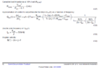
I need the explanation of the following bode plots given in the attached datasheet of UCC28180.
-> Figure 32. Bode Plot of the Current Averaging Circuit
What is the gain at 4.314kHz?
What is current averaging pole?
-> Figure 32. Bode Plot of the Open Voltage Loop without Error Amplifier
Pulse width modulator to power stage pole fPWM_PS = 1.479Hz ------------------------eq (106)
What does it mean?
-> Figure 34. Closed Loop Voltage Bode Plot
The voltage error amplifier is compensated with a zero, fZERO, at the fPWM_PS pole and a pole, fPOLE, placed at 20
Hz to reject high frequency noise and roll off the gain amplitude. The overall voltage loop crossover, fV, is desired
to be at 10 Hz.
What should be the gain and phase at 10Hz.