Continue to Site

Welcome to EDAboard.com

Welcome to our site! EDAboard.com is an international Electronics Discussion Forum focused on EDA software, circuits, schematics, books, theory, papers, asic, pld, 8051, DSP, Network, RF, Analog Design, PCB, Service Manuals... and a whole lot more! To participate you need to register. Registration is free. Click here to register now.

[SOLVED] Shifiting output opamp range between 0V and 10V...

Status
Not open for further replies.

flote21

Advanced Member level 1
Joined
Jan 22, 2014
Messages
411
Helped
1
Reputation
2
Reaction score
3
Trophy points
1,298
Activity points
5,595
Hello everydoby,

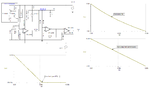
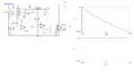
I am trying to shift the minimum Vout1 value to Zero, but I am not able to implement a negative offset in the next thermisto conditioning circuit:

opamp.png

The behaviour I want to achieve is:

1) When R_NTC(min)=166.63Ohm => Vout1=10V
2) When R_NTC(max)=5k => Vout1=0V.

I have achieved the first condition, but I am not able to achieve the second one. How can I get a 0V<=Vout1<=10?

thanks in advance.
 

Read the data sheet.

First of all, I have no idea how this is giving you ANY output. You've got an inverting opamp with a positive input, but a negative opamp supply of zero. Your output should be going negative, but can't with a zero volt supply. Secondly, you need to consider your output swing which is about 3 volts from the rail.
 

Hi,

There are several ways to solve the problem.
My way is to use a difference amplifier circuit.

Klaus
 

I see no negative supplies available. Even with an R-R device, most will get down to about 30-100 mV from zero. If the output needs to go down to 0 V, then that may be a problem.
 
..............

1) When R_NTC(min)=166.63Ohm => Vout1=10V
2) When R_NTC(max)=5k => Vout1=0V.

I have achieved the first condition, but I am not able to achieve the second one......
That's only because you are putting positive voltage into an inverting op amp with a 0V negative supply so the output is at it's minimum and not doing anything. Thus the output positive voltage you are seeing is from the voltage going directly through RG and RF.
If you remove U1, the output will likely be little changed.
 
Hello guys!

Thank you so much for the answers! I am happy to tell you that my previous circuit was totally wrong. I made some big mistakes and it was not possible to achieve the target:

- R_NTC(min)=166.63Ohm => Vout1=10V.
- R_NTC(max)=5k => Vout1=0V.

However with the next circuit it is possible to achieve the previous span to dirve the ADC:

SC_NTC.png

I have run some simulations and it looks working properly:

Simulation for R_NTC(min)=166.63Ohm:

Vout2_166.png

Simulation for R_NTC(max)=5kOhm:

Vout2_5K.png

So I think that this signal conditioning circuit should also work in the real life...do you see anything wrong with it?

Greetings!
 

Hi,

Your circuit now uses three OPAMPs...it looks like you took some effor to get some precision.

some thoughts:
* did you consider linearity? I mean your voltage output range is 0..10V. Did you calculate which temperature generates 5V output?

* NTCs usually are connected to a (long) cable. This cable will cause errors. It will change the resistance you measure and it will introduce some noise. To compensate for the added resistance you may consider three or four wiring system. And for reducing noise I recommend to add some low pass filters.
Now you already added a capacitor next to the NTC. Place it close to the amplifier, not close to the NTC.
Then there is a feedback capacitor across the first OPAMP. Calculate it´s value that fc is much lower than mains frequency for good attenuation.

* use a good PCB layout with solid GND plane. And use ceramics capacitors at the supply coltages.

* there is 5V as NTC supply. If you want precision, then use a reference instead of a voltage regualtor. Additionally I recommedn some low pass filtering of the signal before entering the buffer OPAMP. (is the buffer necessary?). I recommend to connect the 19.5k resistor to the buffer output (instead the buffer input)

* did you consider ESD? Maybe you need some protection circuit.

* if the output drives an ADC, then maybe you need to limit the voltage ... not to destroy the ADC in case of unconnected/shorted NTC.

all in all no big modifications...

Klaus
 

Note that RS=614.62 is not a standard resistor value.

Your circuit will have a very non-linear voltage output versus thermistor resistance.
Perform the simulation varying the R_NTC thermistor value.
Change the value of R_NTC to {R} instead of a fixed value (be sure to use the curly-cue brackets).
Then press the "s" key to generate a Spice directive as follows: .step oct param R 166.63 5000 10.
Perform a DC op pt (.op) to see the output voltage vs. thermistor resistance.

For a linear output, use a constant-current source instead of a constant-voltage through a resistor.

Basic simulation of both sources below:

Capture.PNG
 
Here is a design that includes a 10 V reference and where you have the option of a non-linear or linear transfer function.

If you don't need a linear transfer, then you can omit the current source part and use just the 10k resistor. The switch is only to demonstrate the two options. If your 15 V supply is not exact, then you may have to trim R14 (10k) to calibrate. R4/10 can be a trim pot to adjust the 10 V reference. You only need a few volts for the negative supply to get the opamp down to zero.

It will also limit the output when the NTC goes open.

As a comparison, I include the results for not using a negative rail. It simplifies things a bit if you can tolerate this zero error.
 

Attachments

  • NTC_conv.png
    NTC_conv.png
    56.8 KB · Views: 168
  • NTC_conv_sim.png
    NTC_conv_sim.png
    44.4 KB · Views: 149
Hello KaluST!
Thank you for your tips! One question, when you say:"To compensate for the added resistance you may consider three or four wiring system." You mean, use a Whaetstone bridge instead of the resistor devidier?

thanks!
 

Hi E-Design!

I liked a lot your proposal. But do you think if using a wheatstone bridge combined with your design will improve the measurements?

Thanks in advance!

Here is a design that includes a 10 V reference and where you have the option of a non-linear or linear transfer function.

If you don't need a linear transfer, then you can omit the current source part and use just the 10k resistor. The switch is only to demonstrate the two options. If your 15 V supply is not exact, then you may have to trim R14 (10k) to calibrate. R4/10 can be a trim pot to adjust the 10 V reference. You only need a few volts for the negative supply to get the opamp down to zero.

It will also limit the output when the NTC goes open.

As a comparison, I include the results for not using a negative rail. It simplifies things a bit if you can tolerate this zero error.
 

Status
Not open for further replies.

Similar threads

Part and Inventory Search

Welcome to EDABoard.com

Sponsor

Back
Top