Continue to Site

Welcome to EDAboard.com

Welcome to our site! EDAboard.com is an international Electronics Discussion Forum focused on EDA software, circuits, schematics, books, theory, papers, asic, pld, 8051, DSP, Network, RF, Analog Design, PCB, Service Manuals... and a whole lot more! To participate you need to register. Registration is free. Click here to register now.

I need to calculate the gate current of a pHEMT

Status
Not open for further replies.

skatefast08

Full Member level 3
Joined
Jan 24, 2018
Messages
189
Helped
2
Reputation
4
Reaction score
2
Trophy points
18
Activity points
1,779
I need to calculate the gate current (Igs) using an ATF 54143 transistor for a common source amplifier, because I need to make sure Igs < 1mA. the common source amp has R1 (connected to power supply), R2 (connected to ground), Rd, and Rs. Im trying to figure out the best bias design for a 2.4 GHz microwave amplifier, using this layout form:
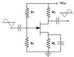
fig20.jpg

[from nptel.ac.in /courses /117107095 /lecturers /lecture_39 /images /fig20.jpg]


In order to get best bias, I think I would need to get close to 1mA for Igs, so I could use the lowest bias resistance (which would decrease noise also).

Vds = 3V, Id = 30mA, Vgs = 0.6V, Vdd = 5v, and need to make sure Igs < 1mA

ATF 54143 datasheet is right here: **broken link removed**


Thanks
 

There isn't such calculation method for pHEMT Gate current.It's even not well modeled yet.
You will take typical measurement values.( or given )
 
I'd expect a lot of process and temperature variability
in the gate Schottky Vf. My only real exposure to this
has been designing T/R element controllers that had
"active bias" amps, sensing drain current and servoing
the gate DC to a reference value. Presumably they
paid my salary plus insane markup because the open
loop biasing is so all-over-the-place as a general rule.

The fact (or datasheet value at least) that gate
-leakage- current can be 0.2mA only adds to the fog.

The back pages of that datasheet have a bunch of
biasing discussion. The pHEMT model has only one
param that looks remotely like a diode Vf (Vgexp=1.91)
which is a not-insane wide bandgap Schottky voltage
but might only be a coincidental match - I couldn't
be bothered to read the MESFETM1 modeling document
or even to search for it, although you certainly could.
 
the gate current, in comparison to the resistor network current, should be almost zero

the fet is a voltage controlled device. are you thinking that it is like a bipolar transistor?

the source resistor/capacitor network you show...works well at low frequencies. but at 2.4 GHz, it is imperative that the source sees a zero impedance to ground. due to chip parasitics, that is unlikely, and any non zero impedance at the source terminal(s) may cause instability
 
Some HEMTs/FETs in some applications are driven to the point
that the gate Schottky goes forward biased. eGaN devices
are one such. In a LNA the bias may favor noise but in a PA
you might favor conductance / current density and driving
down drain capacitance in order to make your gain@freq -
run it hot, is pretty normal in chasing speed.

Another consideration is that RF tends to be low impedances
and the bias network impedance can be under a kOhm with
not much effect to losses, and 1kOhm*0.2mA (spec limit Igg)
would be 200mV of error - probably not worse than the VPO
variation of the FET or the Vf scatter (esp. w/ temp) of the
gate diode.

Low gate impedance also helps noise.
 

Some HEMTs/FETs in some applications are driven to the point
that the gate Schottky goes forward biased. .

generally that is a bad idea for reliability reasons...especially with MOSFETS.
There would also be a ton of phase noise due to trapped carriers when you overdrive the gate....
 

They show in a LNA design using ATF-55143: https://www.rf-microwave.com/resources/products_attachments/5a4386e1891b2.pdf that they use an inductor/transmission line at the source for stability, but you say that it is crucial that it should go straight to ground or it could cause instability. Is using an inductor/transmission line different than using a parallel capacitor and resistor? but if putting an inductor/transmission line at the source, doesn't that increase impedance at the source and hense be more suseptible to instability? just confused, cause Agilent Technologies says the opposite. Or maybe, all nodes have to be transmission lines?

Quick last question, doesn't there need to be a DC gain for the transistor, like BJT's? because I know when you increase DC gain for BJT's the better overal AC gain you get.
 

you DO realize that the ATF55143 is a mesfet, NOT a jfet as you had drawn.

Also note the Widlar Current Mirror in the biasing part of the circuit on that data sheet....

putting small inductances in the drain to source....that can easily be modeled and checked to see if it helps, or hurts, stability and NF. I would suggest you do that.
 
What if I just put the source to the ground without anything in between? how significant of a change would the circuit be affected without the inductor/transmission line at the source? since you said before "but at 2.4 GHz, it is imperative that the source sees a zero impedance to ground." couldn't I just give the source a direct path to ground, and I would still get ok stability and gain?

All I care is that I get good stability (I am just testing from an input and output termination of 50 ohms) and good gain. I dont care about NF right now, cause I am not interested in that right now.

If you have time for another question, I was wondering how did Agilent get the matching network design for L1/C1 and L4/C4 (from: **broken link removed** because when I do a bilateral match (while I keep stability circles outside and tangent to the smith chart, which is best when designing bilateral matching circuit, correct?) I do not get component values that are anything close to what their values were for L1/C1 and L4/C4, why would this be?

thanks
 

i personally have NEVER gotten away with putting anything between the source lead(s) and the ground via holes above 2 GHz in a microstrip circuit. Maybe it can be done...it certainly can be done if you are doing it on an IC.

IF you do not have a DC resistor between the source and ground, there is no biasing feedback mechanism. Maybe you can live with that....maybe you need to add an active bias network in the DC part of the circuit (pass transistors, op amps, etc).

It is called "engineering", to make a complete design you have to take into account ALL of this stuff...temperature drift, manufacturing tolerances and repeatibility in your FET devices, and so on.
 

Status
Not open for further replies.

Part and Inventory Search

Welcome to EDABoard.com

Sponsor

Back
Top