sgrjuneja
Newbie level 5
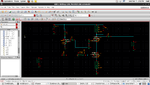
I am designing LNA for GPS application (1.57GHz) using cadence virtuoso (IC616) and Spectre (MMSIM131) tool. Circuit is attached.
My topology is inductive source degeneration. I am able to match the input and output of LNA to 50 Ohms input and output port respectively with S11 = -18dB and S22 = -10dB. My noise figure is 2.4dB at the frequency of interest.
But the problem is I am not been able to get any gain out of the circuit. My S21 is always coming equal to S22 and it is -2.5dB. Please help me understand what could possibly be wrong with the circuit.
DC parameters/bias points for my gain transistor are as follows:-
Gate Over Drive Voltage - 0.12V, Id = 5.69A, Vgs = .608V, Vds = .605V, Vth = .558V, gm = 81m, gds = 2.14m, Cgs = 548Ff