musmanm
Member level 2
Hello everyone
I'm using a few different microstrip calculators, but when I draw my trace, the suggested width (2.77mm) seems huge.
Calculator here: http://www.rfdh.com/
The transmission line needs to be 50 ohms as it connects directly with a 50 ohm matched impedance IC, of which the leads are around 0.3mm or even smaller.
I'm using FR4 and this is a 2-layer board
dielectric constant er is 4.5
Frequency of operation (3 to 6 GHz)
strip thickness is 1 oz copper, 0.035mm
dielectric height is a standard 2 layer board, it is 1.6mm
I need a Z0 of 50 ohms transmission line.
What am I doing wrong?
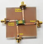
I recently fabricated a directional coupler, to be used in my system. I kept 2.77mm width and it did not give me good results, results are very strange.
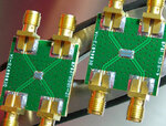
And I googled some directional coupler PCBs and their evaluation boards, they under 4-8GHz are using a very thin trace. How the width became so thin/narrow if that also is a 50 ohm tx line?
I am attaching my fabricated directional coupler and also the Google samples.
Please see my fabricated directional coupler with 2.77mm (50ohm) trace width below:

and the googled directional coupler samples are:

Need an advise on how can I make a thinner/narrower 50ohm width to fabricate my directional coupler with minimum losses.
Thanks!
I'm using a few different microstrip calculators, but when I draw my trace, the suggested width (2.77mm) seems huge.
Calculator here: http://www.rfdh.com/
The transmission line needs to be 50 ohms as it connects directly with a 50 ohm matched impedance IC, of which the leads are around 0.3mm or even smaller.
I'm using FR4 and this is a 2-layer board
dielectric constant er is 4.5
Frequency of operation (3 to 6 GHz)
strip thickness is 1 oz copper, 0.035mm
dielectric height is a standard 2 layer board, it is 1.6mm
I need a Z0 of 50 ohms transmission line.
What am I doing wrong?
I recently fabricated a directional coupler, to be used in my system. I kept 2.77mm width and it did not give me good results, results are very strange.
And I googled some directional coupler PCBs and their evaluation boards, they under 4-8GHz are using a very thin trace. How the width became so thin/narrow if that also is a 50 ohm tx line?
I am attaching my fabricated directional coupler and also the Google samples.
Please see my fabricated directional coupler with 2.77mm (50ohm) trace width below:

and the googled directional coupler samples are:

Need an advise on how can I make a thinner/narrower 50ohm width to fabricate my directional coupler with minimum losses.
Thanks!