naveennamboothiri
Newbie level 3
Hi everyone,
I need a clarification regarding differential routing for isolated RJ45
How to achieve differential trace impedance for isolated RJ45 signals in PCB? Even if it is 4layer there should not be any ground/power plane under the differential pairs after magnetics.
• Can we give shield ground of RJ45 connector as reference plane for these differential traces to achieve 100ohm impedance for differential traces on the PCB? If so how can we achieve the 2KV isolation between differential pair and shield ground?
• How can we achieve the differential impedance without reference plane and by using only trace width, separation and dielectric permittivity? Without using dielectric height (H) since no plane here.
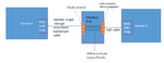
I have attached an image which shows system level requirement
I need a clarification regarding differential routing for isolated RJ45
How to achieve differential trace impedance for isolated RJ45 signals in PCB? Even if it is 4layer there should not be any ground/power plane under the differential pairs after magnetics.
• Can we give shield ground of RJ45 connector as reference plane for these differential traces to achieve 100ohm impedance for differential traces on the PCB? If so how can we achieve the 2KV isolation between differential pair and shield ground?
• How can we achieve the differential impedance without reference plane and by using only trace width, separation and dielectric permittivity? Without using dielectric height (H) since no plane here.
I have attached an image which shows system level requirement