Continue to Site

Welcome to EDAboard.com

Welcome to our site! EDAboard.com is an international Electronics Discussion Forum focused on EDA software, circuits, schematics, books, theory, papers, asic, pld, 8051, DSP, Network, RF, Analog Design, PCB, Service Manuals... and a whole lot more! To participate you need to register. Registration is free. Click here to register now.

Boost converter push pull topology

Status
Not open for further replies.

ShayanZulfiqar

Junior Member level 1
Joined
Oct 23, 2017
Messages
16
Helped
0
Reputation
0
Reaction score
0
Trophy points
1
Activity points
123
Hello everyone,
I am currently designing a boost converter based on push pull topology. I am attaching the link to the schematic. The problem is that when i check the wave at the drain of either of the mosfet then the positve peak of the square wave has alot of noise. The peak of square wave is like a exponentially decaying sine wave. Kindly tell me why this is happening and how to solve it.

Link to schematic: https://tahmidmc.blogspot.com/2013/01/using-sg3525-pwm-controller-explanation.html?m=1
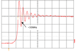
 

Do you mean like this?
Ring.png

RC snubber across each FET could help.
 

In Tahmid's blog there is mention / question re the need
for snubbers. The reply focused on the FET stress and
neglected the ringing / EMI concern. Abrupt dI/dt or dV/dt
(and you have both) will kick the tank (Coss of FET, and
some inductance term(s) of the xfmr primary) and nothing
to scrub off that energy.

Another push-pull concern is "flux walk" which comes from
leg-leg circuit imbalances such as on-time, component
mismatches etc. More sophisticated controllers may have
features to sense and correct that, otherwise be sure to
leave yourself plenty of core saturation margin and maybe
a soft saturation characteristic (i.e. no "cliff").
 

Last edited by a moderator:

One thing i dont understand is that how the output DC voltage is increased by varying the duty cycle. I get that the RMS will vary but the rectifier will just convert the -ve portion into +ve of same amplitude
When Q1 ON --> secondary of xformer =Vin/N
When Q1 OFF --> secondary of xformer=0
When Q2 ON --> secondary of xformer= -Vin/N
When Q2 OFF --> secondary of xformer =0
---Cycle repeats--

One thing to notice is that the output filter inductor sees 2 times the frequency of the signal applied to the xformer, then, the filter inductor sees a square wave between Vin/N and 0. (N=N1/N2)

- - - Updated - - -

When duty cycle=50% (in practice one should go a bit less depending of switching times of transistors... e.g. 49%, 48% ...), you get what you are saying i.e. the output voltage rectified "Vin/N".
 

Status
Not open for further replies.

Similar threads

Part and Inventory Search

Welcome to EDABoard.com

Sponsor

Back
Top