Continue to Site

Welcome to EDAboard.com

Welcome to our site! EDAboard.com is an international Electronics Discussion Forum focused on EDA software, circuits, schematics, books, theory, papers, asic, pld, 8051, DSP, Network, RF, Analog Design, PCB, Service Manuals... and a whole lot more! To participate you need to register. Registration is free. Click here to register now.

is there anyone assembler here???need help regarding max7219 coding...

Status
Not open for further replies.

peter002

Member level 3
Joined
Mar 18, 2013
Messages
56
Helped
0
Reputation
0
Reaction score
0
Trophy points
1,286
Location
Hindusthaan
Activity points
1,765
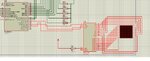
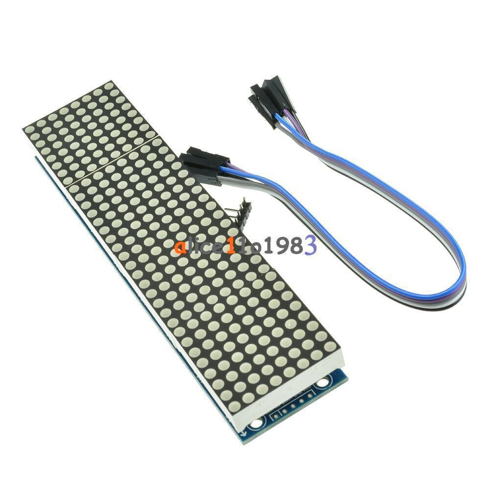
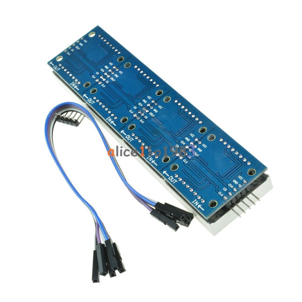
hello al, i m trying to program mcu to run max7219 that i bought online with matrix soldered already...below is my code IN THE ATTACHMENT, plz chk and let me know where i m wrong??? i m not able to to turn it on at all, in proteus i can see data at DOUT but the matrix doesnt works at all, all leds are on in the proteus and no change can be seen on the matrix or the 7219 pins.. in practical my module does nothing.... plz hlp me..
thanx in advanc
 

Attachments

  • new.txt
    8.7 KB · Views: 60

I can't open the attachment, can you post it as formatted code please. Copy the source code into the message box then just before it, type '[ C O D E ]' without the quote marks and spaces. Just after it type '[ / C O D E ]' again without the quotes or spaces. When you post the message it will preserve the original formatting. Make sure you tell us which processor and assembler you are using.

Brian.

[edit]
I managed to read the file - i have not followed the code fully but are you sure the character table should be in EEPROM and if so, where is the EEPROM read routine?
Possibly 'DE' should be a different storage directive.

Brian.
 

thanx for your reply bro, i m storing the character set bit patterns in the flash storage, at they are working very well becoz i have made the led sign board previously and read the patterns from the flash storage....

but but but for the time right now i have made a sub routine named as "SENDA" that i used to send the charater set or a directly to the max7219.. just for the test purpose...

the DE command write the dta to the flash store of the mcu

here is the SENDA routine...

Code:
SENDA		MOVLW	D'1'
		MOVWF	REGVALUE
		MOVLW	D'126'
		MOVWF	DTVALUE
		CALL	MAX7219SPI
		INCF	REGVALUE,F
		MOVLW	D'9'
		MOVWF	DTVALUE
		CALL	MAX7219SPI
		INCF	REGVALUE,F
		MOVLW	D'9'
		MOVWF	DTVALUE
		CALL	MAX7219SPI
		INCF	REGVALUE,F
		MOVLW	D'9'
		MOVWF	DTVALUE
		CALL	MAX7219SPI
		INCF	REGVALUE,F
		MOVLW	D'9'
		MOVWF	DTVALUE
		CALL	MAX7219SPI
		INCF	REGVALUE,F
		MOVLW	D'126'
		MOVWF	DTVALUE
		CALL	MAX7219SPI
		RETURN
BTW i m using 16f876a and the ssembler is MPASMWIN.EXE...
THAT I VE BEEN USING FROM YEAR WITHOUT ANY ERROR
 
Last edited:

Your code isn't particularly efficient, it would be be smaller and less complicated if you rotated the mask bit (TMPBIN) once then called a routine to set or reset the data line instead of rotating it in both routines.

However, and I have not attempted to assemble it or test it, I think the bug might be in the "ONEE" routine, if the last data bit isn't a '1' it doesn't set the 'LOAD' pin to latch data to the 7219. You really only want to set LOAD when MAXTMP is zero, regardless of the data bit being sent.

If you do as I suggest, there will only be one place you check if all the bits are sent so there is no risk of not setting or prematurely setting the LOAD signal.

Brian.
 

ok, in max7219 whats the procedure to lath the data, means before sending data do i need to clear the load pin and after the all bits are sent do i need to pul it high to latch the data???
and plz can u explain a bit more about your first line??.. i have to send the register address first and then data... so i have to use the tmpbin on both places in diff values...
what do you suggest that i cud have done to make my code more easy..
thanx bro..

- - - Updated - - -

Code:
MAX7219SPI    MOVLW    D'8'
        MOVWF    MAXTMP
        MOVLW    B'00001000'
        MOVWF    TMPBIN
        BCF    LOAD
AS        MOVF    REGVALUE,W
        ANDWF    TMPBIN,W
        
        BTFSS    STATUS,Z
        GOTO    OONE
        GOTO    ZERO

OONE        BSF    DIN
        CALL    PULSECLK
        RRF    TMPBIN,F
        DECFSZ    MAXTMP,F
        GOTO    AS
        GOTO    NEXT

ZERO        BCF    DIN
        CALL    PULSECLK
        RRF    TMPBIN,F
        DECFSZ    MAXTMP,F
        GOTO    AS
        GOTO    NEXT

NEXT        MOVLW    D'8'
        MOVWF    MAXTMP
        MOVLW    B'10000000'
        MOVWF    TMPBIN
AAS        MOVF    DTVALUE,W
        ANDWF    TMPBIN,W
        
        BTFSS    STATUS,Z
        GOTO    ONEE
        GOTO    ZEROO

ONEE        BSF    DIN
        CALL    PULSECLK
        RRF    TMPBIN,F
        DECFSZ    MAXTMP,F
        GOTO    AAS
        BSF    LOAD
        RETURN

ZEROO        BCF    DIN
        CALL    PULSECLK
        RRF    TMPBIN,F
        DECFSZ    MAXTMP,F
        GOTO    AAS
        BSF    LOAD
        RETURN

HOWS THAT ROUTINE NOW???? BUT IN PROT STILL SAME RESPONSE...

- - - Updated - - -

one strange thing found, that if disconnec the cs/load wire from the breadboard the matrixes starts to show garbage data passing by, but if i connects it again then the display hangs and if i reset chip while load wire connected the matrixes again doesnt shows anything....

- - - Updated - - -

as i said i m trying to send the bit pattern of a but i m getting garbage values on matrixes.. and they r displayed only if the load pin is disconnected.. in practicle i m getting those responses but in prot i m getting nothing...
 

It works like this:
1. make CLK and CS/LOAD low. This tells the IC that 16 bits of data are about to arrive.
2. put bit 15 on DIN then make the CLK high. After at least 50nS, make the CLK line low again.
3. repeat step 2 for bits 14, 13....0.
4. make CS/LOAD high. This tells the IC that the 16 bits have been received and are ready to use.

I think that by disconnecting CS/LOAD you could see the effect of the bits being shifted in instead of waiting for them all to arrive.

The better way to code it is like this:
1. set your bit counter with 8
2. rotate the data left so the MSB is put in the 'C' carry flag
3. test the carry flag (btfss STATUS,C) and set or reset the DIN pin
4. decrement the bit counter and go back to step 2 if it isn't zero

If you make that a subroutine, you can use it twice, first to send D15-D8 then again to send D7-D0, just load the register address or the LED data each time.

Brian.
 

Would you be willing to post a circuit diagram of how you have connected the PIC16F876A to the MAX7219?
 

HEY BRO, i modified my max7219 spi routine.. plz take a look...
Code:
SPI7219        MOVLW    D'8'        ;SPI BIT BANGING ROUTINE
        MOVWF    MAXTMP
AS        BCF    CLK
        MOVF    TMPVALUE,W
        ANDWF    TMPBIN,W
        
        BTFSS    STATUS,Z
        GOTO    OONE
        GOTO    ZERO

OONE        BSF    DIN
        BSF    CLK
        RRF    TMPBIN,F
        CALL    MAXDEL
        DECFSZ    MAXTMP,F
        GOTO    AS
        RETURN

ZERO        BCF    DIN
        BSF    CLK
        RRF    TMPBIN,F
        CALL    MAXDEL
        DECFSZ    MAXTMP,F
        GOTO    AS
        RETURN

MAX7219SPI    MOVLW    B'00001000'
        MOVWF    TMPBIN
        BCF    LOAD
        MOVF    REGVALUE,W
        MOVWF    TMPVALUE
        CALL    SPI7219

        MOVLW    B'10000000'
        MOVWF    TMPBIN
        MOVF    TMPVALUE,W
        MOVWF    DTVALUE
        CALL    SPI7219
        BCF    LOAD
        RETURN
it really made the code easier, i have even modified the clk pulsing function in that routine.. hope you find it better now... will post the matrix new response soon

here is the connection ckt..

- - - Updated - - -

what ever i do in the code, i didnt get any change in the proteus... wen i ran the simulation i found aall leds of matrix turned on the found no chaange on the output pins of the max7219..

here is my modified new code
 

Attachments

  • Untitled.jpg
    Untitled.jpg
    206.7 KB · Views: 73
  • new1.txt
    9.2 KB · Views: 61
Last edited by a moderator:

I think you are using the PIC16F876A MCU> That MCU as an SPI interface (in the MSSP peripheral).
It also seems to be that you are bit-banging the SPI signals to the MAX7219. (I must admit to not really understanding assembler - I gave up on that in the 8008 days.)
Would it not be a whole lot simpler to use the SPI hardware?
Susan

yep bro, tat wud be best but i m planning to use the module with the pic 16f628 that doesnt uses the mmsp spi, it doesnt hav the spi hardware installed in the pic, so i m trying to use the bit banging method to communicate with the chip
 

(I must admit to not really understanding assembler - I gave up on that in the 8008 days.)
Giving your age away 'Bro' Susan! (I know because I programmed 8008 too)

We really need to see the whole program peter002, it still looks far from optimal and I can't see why you use 'rrf' twice when it only needs doing once.
I think this will do everything in your code but I am not at an assembler at the moment so it is written from my memory:
Code:
Send_8_bits
    movwf shiftreg      ;save the SPI data for later
    movlw 8             ;this is how many bits to shift out
    movwf shiftcount    ;variable to hold remaining shifts
shift_loop
    bcf DIN             ;7219 data line = 0
    rlf shiftreg,f      ;shift MSB into carry flag
    btfsc STATUS,C      ;skip next instruction if MSB was 0
    bsf DIN             ;MSB was 1 so make DIN = 1
    nop                 ;just a delay
    bsf CLK             ;clock to 7219 = 1
    nop                 ;just a delay
    bcf CLK             ;clock to 7219 = 0
    decfsz shiftcount,f ;see if more bits to send
    goto shift_loop
    return

You use it like this:
bcf LOAD ;start the transfer
put the register address in W
call 'send_8_bits'
put the data in W
call 'send_8_bits'
bsf LOAD ;end the transfer.

As I stress, I'm writing this while on a train at the moment and I do not have a PC to run an assembler so it isn't tested but it shows how you can simplify the program.

Brian.


your given example seems very interesting bro, getting upto it, i have made new routines in my code.. plz chk my new code from my previous post that is named as "new1.txt"

- - - Updated - - -

i am using the rrf command because the msb has to be sent first to the 7219, so i am anding the value IN REGVALUE with 10000000 so 8TH bit is tested and sent to the max7219 first and the the binary balue get rrf so it becomes 01000000 and anded again and this time the 7th bit is testd for 1 or 0 and again rrf maked the tmpbin 00100000 nd the 6th bit is tested and so on...
as i think to send the msb first and the lsb in last i hav use the rrf command .... correct me is i m wrong bro..

- - - Updated - - -

i chked your code bro, and its quite interesting, you do not need to and the data, you are simply rotating the data value left and checking for the carry bit to be set ot unset, if the left shifted byte had the 1 at msb place then the carry flag vl be set but there was a 0 then carry flag vl be 0.. am i right bro???

- - - Updated - - -

hey brian, after using your routine it sharted to show sm changes on the output pins of the max7219... trying to get it to display smting usefull, willl post soon again...

- - - Updated - - -

hey brian, after using your routine it sharted to show sm changes on the output pins of the max7219... trying to get it to display smting usefull, willl post soon again...
 

i chked your code bro, and its quite interesting, you do not need to and the data, you are simply rotating the data value left and checking for the carry bit to be set ot unset, if the left shifted byte had the 1 at msb place then the carry flag vl be set but there was a 0 then carry flag vl be 0.. am i right bro???
Basically yes. It doesn't matter if the data you are sending is destroyed by the routine because you only need it once. That makes it safe to rotate it through the carry flag and test the C flag to tell if it was a 1 or 0. Note that I make DIN = 0 before checking the carry flag, if carry is 0 it stays at zero, otherwise DIN = 1. It saves a variable and some instructions to do it that way. The level on the DIN line only matters at the time CLK goes high so it doesn't care if DIN is changed to zero and back again if you are sending consecutive 1's.

It works your way too, it is called a 'bit mask' when you move a bit along a variable then AND it with another variable but it is slower and uses more memory.

Brian.
 
@peter002,

It seems to me that there are several areas of you code that could be better organized.

Please see if this code will work in your setup.
Code:
;
;                            PIC16F877A
;                    +-----------:_:-----------+
;         ICD_VPP -> :  1 MCLRn         PGD 28 : <> RB7 ICD_PGD
;             RA0 <> :  2 AN0           PGC 27 : <> RB6 ICD_PGC
;             RA1 <> :  3 AN1               26 : <> RB5
;             RA2 <> :  4 AN2               25 : <> RB4
;             RA3 <> :  5 AN3           PGM 24 : <> RB3
;             RA4 <> :  6 T0CKI             23 : <> RB2
;             RA5 <> :  7 AN4/SS            22 : <> RB1
;             GND <> :  8 VSS          INT0 21 : <> RB0
;      20MHz XTAL -> :  9 OSC1          VDD 20 : <- 5v0
;      20MHz XTAL <- : 10 OSC2          VSS 19 : <- GND
;      LCD_RS RC0 -> : 11 T1OSO          RX 18 : <> RC7
;      LCD_E  RC1 <> : 12 T1OSI          TX 17 : <> RC6
; MAX7219_DI  RC2 <> : 13 CCP1          SDO 16 : <> RC5 MAX7219_CLK
;             RC3 <> : 14 SCK/SCL   SDA/SDI 15 : <> RC4 MAX7219_CSn
;                    +-------------------------+
;                              DIP-28
;
        LIST    r=dec, n=0, c=160
        errorlevel -302         ; Suppress the not in bank zero warning
#INCLUDE "P16F876A.INC"


;MACROS


        __CONFIG        _BODEN_OFF & _CP_OFF & _CPD_OFF &_WRT_OFF & _PWRTE_OFF & _WDT_OFF & _LVP_OFF & _HS_OSC & _DEBUG_OFF

        LIST    P=16F876A

#define BANK0   H'000'
#define BANK1   H'080'
#define BANK2   H'100'
#define BANK3   H'180'

;RTC DEFINES---------------
#DEFINE DIN     PORTC,2
#DEFINE CLK     PORTC,5
#DEFINE LOAD    PORTC,4
;RTC DEFINES END-----------


;VARIABLES-------------------------
        CBLOCK  H'20'

SPI_TEMP
CHAR_TO_SEND

        ENDC


        ORG     0
                NOP
                GOTO    RESET


;MAX7219 SUBS----------------------------------------------------------------------------------
;
; Function: BB_SPI_TX
;
; Description:
;   Bit-Bang SPI transmit function.
;
; Input:    WREG = 8-bit to send to SPI device
;
; Output:   none
;
; Uses:     SPI_TEMP
;
#define SPI_MOSI_MASK (B'00000100')
BB_SPI_TX:
                MOVWF   SPI_TEMP
                RLF     SPI_TEMP,W
                XORWF   SPI_TEMP,F
                BSF     SPI_TEMP,0
                MOVLW   SPI_MOSI_MASK
                BCF     DIN             ; Clear PORTC bit 2
BB_SPI_TX1:
                BCF     CLK
                BTFSC   STATUS,C
                XORWF   PORTC,F         ; Update MOSI output bit
                BCF     STATUS,C
                RLF     SPI_TEMP,F
                BSF     CLK
                MOVF    SPI_TEMP,F
                BTFSS   STATUS,Z
                GOTO    BB_SPI_TX1
                BCF     CLK
                RETURN

;
; Function: SEND_ASCII
;
; Description:
;   Lookup ASCII character in 5x7 character generator table in code space
;   and send pattern to MAX7219.
;
; Input:    WREG = ASCII character.
;
; Output:   none
;
; Uses:
;
; Calls:    CG_SET_ADDRESS, CG_LOOK_UP, BB_SPI_TX
;
SEND_ASCII:
                CALL    CG_SET_ADDRESS

                CALL    MAX7219_SELECT
                MOVLW   D'2'            ; Row 1 of 5x7 pattern
                CALL    BB_SPI_TX
                CALL    CG_LOOK_UP      ; Send data
                CALL    BB_SPI_TX
                CALL    MAX7219_DESELECT

                CALL    MAX7219_SELECT
                MOVLW   D'3'            ; Row 2 of 5x7 pattern
                CALL    BB_SPI_TX
                CALL    CG_LOOK_UP      ; Send data
                CALL    BB_SPI_TX
                CALL    MAX7219_DESELECT

                CALL    MAX7219_SELECT
                MOVLW   D'4'            ; Row 3 of 5x7 pattern
                CALL    BB_SPI_TX
                CALL    CG_LOOK_UP      ; Send data
                CALL    BB_SPI_TX
                CALL    MAX7219_DESELECT

                CALL    MAX7219_SELECT
                MOVLW   D'5'            ; Row 4 of 5x7 pattern
                CALL    BB_SPI_TX
                CALL    CG_LOOK_UP      ; Send data
                CALL    BB_SPI_TX
                CALL    MAX7219_DESELECT

                CALL    MAX7219_SELECT
                MOVLW   D'6'            ; Row 5 of 5x7 pattern
                CALL    BB_SPI_TX
                CALL    CG_LOOK_UP      ; Send data
                CALL    BB_SPI_TX
                CALL    MAX7219_DESELECT

                RETURN
;
; Function: CG_SET_ADDRESS
;
; Description:
;   Set address for character generator lookup.
;   Multiply the ASCII character code by 5 and
;   add the based address of the look up table.
;
; Input:    WREG = 8-bit to send to SPI device
;
; Output:   EEADRH:EEADR set to first byte of data
;
CG_SET_ADDRESS:
                banksel BANK2
                MOVWF   EEADR
                CLRF    EEADRH
                CLRC
                RLF     EEADR,F
                RLF     EEADRH,F
                RLF     EEADR,F
                RLF     EEADRH,F
                ADDWF   EEADR,F
                BTFSC   STATUS,C
                INCF    EEADRH,F
                MOVLW   LOW(ASCII_CHAR_GEN)
                ADDWF   EEADR,F
                BTFSC   STATUS,C
                INCF    EEADRH,F
                MOVLW   HIGH(ASCII_CHAR_GEN)
                ADDWF   EEADRH,F
                banksel BANK0
                RETURN
;
; Function: CG_LOOK_UP
;
; Input:        Code space address in EEADRH:EEADR
;
; Output:       WREG = Low 8-bit at address
;               EEADRH:EEADR incremented
;
CG_LOOK_UP:
                banksel BANK3           ; Bank 3
                BSF     EECON1,EEPGD    ; Point to PROGRAM memory
                BSF     EECON1,RD       ; EE Read
                NOP                     ; 2-cycle wait
                NOP                     ; to read code space
                banksel BANK2
                MOVF    EEDATA,W        ; W = low 8-bits of data in program space
                INCF    EEADR,F         ; Increment to next address
                BTFSC   STATUS,Z
                INCF    EEADRH,F
                banksel BANK0
                RETURN
;
; Assert the SPI chip select for the MAX7219
;
MAX7219_SELECT:
                BCF     LOAD
                RETURN
;
; Deassert the SPI chip select for the MAX7219
;
MAX7219_DESELECT:
                BSF     LOAD
                NOP
                NOP
                NOP
                RETURN

;
; Function: MAX7219INIT
;
; Description:
;   Initialize MAX7219 LED Display driver
;
; Input:    none
;
; Output:   none
;
; Calls:    BB_SPI_TX, MAX7219_DESELECT
;
MAX7219INIT:
                CALL    MAX7219_DESELECT
                BCF     CLK

                CALL    MAX7219_SELECT
                MOVLW   H'0C'           ;SHUTDOWN COMMAND
                CAll    BB_SPI_TX
                MOVLW   H'01'           ;RELEASED
                CAll    BB_SPI_TX
                CALL    MAX7219_DESELECT

                CALL    MAX7219_SELECT
                MOVLW   H'09'           ;DECODE MODE COMMAND
                CAll    BB_SPI_TX
                MOVLW   D'0'            ;DISABLED FOR ALL DIGITS
                CAll    BB_SPI_TX
                CALL    MAX7219_DESELECT

                CALL    MAX7219_SELECT
                MOVLW   H'0A'           ;INTENSITY COMMAND
                CAll    BB_SPI_TX
                MOVLW   H'05'           ;INTENSITY VALUE
                CAll    BB_SPI_TX
                CALL    MAX7219_DESELECT

                CALL    MAX7219_SELECT
                MOVLW   H'0B'           ;SCAN LIMIT COMMAND
                CAll    BB_SPI_TX
                MOVLW   H'07'           ;ALL DIGITS
                CAll    BB_SPI_TX
                CALL    MAX7219_DESELECT

                CALL    MAX7219_SELECT
                MOVLW   H'0F'           ;TEST MODE COMMAND
                CAll    BB_SPI_TX
                MOVLW   D'0'            ;NORMAL
                CAll    BB_SPI_TX
                CALL    MAX7219_DESELECT

                RETURN


;MAX7219 SUBS ENDS-----------------------------------------------------------------------------
INIT
                CLRF    INTCON          ;DISABLE INTERUPTS
                CLRF    STATUS
                MOVLW   B'00000111'     ;DISABLE COMPS.
                MOVWF   CMCON           ;
                banksel BANK1           ;SELECT BANK1
                                        ;Disable pull-ups
                                        ;INT on rising edge
                                        ;TMR0 clock source is FOSC/4
                                        ;TMR0 Incr low2high trans.
                                        ;Prescaler assign to Timer0
                                        ;Prescaler rate is 1:256
                MOVLW   B'11010111'     ;Set PIC options (See datasheet).
                MOVWF   OPTION_REG      ;Write the OPTION register.
                MOVLW   D'6'
                MOVWF   ADCON1          ;SET PORT A AS DIGITAL I/O'S NOT AS AD CVONVERTORS
                                        ;START UP AS A/D PINS NOT AS DIGITAL I/O PINS WHY ?
                MOVLW   B'11000000'     ;
                MOVWF   TRISB           ;ALL PORT B OUTPUTS EXCEPT RB7 AND RB6, USED FOR ICD
                MOVLW   B'11000000'
                MOVWF   TRISC           ;ALL PORT C OUTPUTS EXCEPT RC7 AND RC6 USED FOR USART
                MOVLW   B'11011111'     ;ALL PORT A INPUTS  EXCEPT RA5
                MOVWF   TRISA
                banksel BANK0           ;SELECT BANK0
                CLRF    PORTB           ;PORTB CLEAR
                CLRF    PORTC           ;PORTC CLEAR
                MOVLW   B'00100000'     ;ASSERT MAX7219 LOAD PIN TO HIGH
                MOVWF   PORTA           ;PORTA CLEAR

                RETURN                  ;END OF SUB
;
; Function: DELAY
;
; Description:
;   Use TIMER0 to count cycles for a delay.
;
;   Delay: (4 * PRESCAL_VALUE * TIMER0_COUNT * WREG) / FOSC
;          (4 * 256           * 256          * 76  ) / 20000000 = 0.9961472 seconds
;
DELAY:
                MOVLW   D'76'
                BCF     INTCON,TMR0IF
DELAY_1:
                BTFSS   INTCON,TMR0IF
                GOTO    DELAY_1
                BCF     INTCON,TMR0IF
                ADDLW   -1
                BTFSS   STATUS,Z
                GOTO    DELAY_1
                RETURN

;------------------------------------------------------------------------------------------

RESET:
                CALL    INIT
                CALL    MAX7219INIT
SHOW_START:
                MOVLW   '!'
                MOVWF   CHAR_TO_SEND
SHOW_LOOP:
                MOVF    CHAR_TO_SEND,W
                CALL    SEND_ASCII
                CALL    DELAY
                INCF    CHAR_TO_SEND,F
                MOVLW   D'132'
                XORWF   CHAR_TO_SEND,W
                BTFSS   STATUS,Z
                GOTO    SHOW_LOOP
                GOTO    SHOW_START

;
; Reserved the last 0x500 instruction words (0x1B00 to 0x1FFF)
; of code space in page 3 for the ASCII character generator table.
;
        ORG     H'1B00'

ASCII_CHAR_GEN:
                DW      B'00000000',B'00000000',B'00000000',B'00000000',B'00000000'  ;ASCII 0x00
                DW      B'00000000',B'00000000',B'00000000',B'00000000',B'00000000'  ;ASCII 0x01
                DW      B'00000000',B'00000000',B'00000000',B'00000000',B'00000000'  ;ASCII 0x02
                DW      B'00000000',B'00000000',B'00000000',B'00000000',B'00000000'  ;ASCII 0x03
                DW      B'00000000',B'00000000',B'00000000',B'00000000',B'00000000'  ;ASCII 0x04
                DW      B'00000000',B'00000000',B'00000000',B'00000000',B'00000000'  ;ASCII 0x05
                DW      B'00000000',B'00000000',B'00000000',B'00000000',B'00000000'  ;ASCII 0x06
                DW      B'00000000',B'00000000',B'00000000',B'00000000',B'00000000'  ;ASCII 0x07
                DW      B'00000000',B'00000000',B'00000000',B'00000000',B'00000000'  ;ASCII 0x08
                DW      B'00000000',B'00000000',B'00000000',B'00000000',B'00000000'  ;ASCII 0x09
                DW      B'00000000',B'00000000',B'00000000',B'00000000',B'00000000'  ;ASCII 0x0A
                DW      B'00000000',B'00000000',B'00000000',B'00000000',B'00000000'  ;ASCII 0x0B
                DW      B'00000000',B'00000000',B'00000000',B'00000000',B'00000000'  ;ASCII 0x0C
                DW      B'00000000',B'00000000',B'00000000',B'00000000',B'00000000'  ;ASCII 0x0D
                DW      B'00000000',B'00000000',B'00000000',B'00000000',B'00000000'  ;ASCII 0x0E
                DW      B'00000000',B'00000000',B'00000000',B'00000000',B'00000000'  ;ASCII 0x0F
                DW      B'00000000',B'00000000',B'00000000',B'00000000',B'00000000'  ;ASCII 0x10
                DW      B'00000000',B'00000000',B'00000000',B'00000000',B'00000000'  ;ASCII 0x11
                DW      B'00000000',B'00000000',B'00000000',B'00000000',B'00000000'  ;ASCII 0x12
                DW      B'00000000',B'00000000',B'00000000',B'00000000',B'00000000'  ;ASCII 0x13
                DW      B'00000000',B'00000000',B'00000000',B'00000000',B'00000000'  ;ASCII 0x14
                DW      B'00000000',B'00000000',B'00000000',B'00000000',B'00000000'  ;ASCII 0x15
                DW      B'00000000',B'00000000',B'00000000',B'00000000',B'00000000'  ;ASCII 0x16
                DW      B'00000000',B'00000000',B'00000000',B'00000000',B'00000000'  ;ASCII 0x17
                DW      B'00000000',B'00000000',B'00000000',B'00000000',B'00000000'  ;ASCII 0x18
                DW      B'00000000',B'00000000',B'00000000',B'00000000',B'00000000'  ;ASCII 0x19
                DW      B'00000000',B'00000000',B'00000000',B'00000000',B'00000000'  ;ASCII 0x1A
                DW      B'00000000',B'00000000',B'00000000',B'00000000',B'00000000'  ;ASCII 0x1B
                DW      B'00000000',B'00000000',B'00000000',B'00000000',B'00000000'  ;ASCII 0x1C
                DW      B'00000000',B'00000000',B'00000000',B'00000000',B'00000000'  ;ASCII 0x1D
                DW      B'00000000',B'00000000',B'00000000',B'00000000',B'00000000'  ;ASCII 0x1E
                DW      B'00000000',B'00000000',B'00000000',B'00000000',B'00000000'  ;ASCII 0x1F
                DW      B'00000000',B'00000000',B'00000000',B'00000000',B'00000000'  ;SPACE ASCII DEC 32
                DW      B'00000000',B'00000000',B'01011111',B'00000000',B'00000000'  ;!
                DW      B'00000000',B'00000111',B'00000000',B'00000111',B'00000000'  ;"
                DW      B'00010100',B'01111111',B'00010100',B'01111111',B'00010100'  ;#
                DW      B'00100100',B'00101010',B'01111111',B'00101010',B'00010010'  ;$
                DW      B'00100011',B'00010011',B'00001000',B'01100100',B'01100010'  ;%
                DW      B'00110110',B'01001001',B'01010101',B'00100010',B'01010000'  ;&
                DW      B'00000000',B'00000000',B'00000011',B'00000000',B'00000000'  ;'
                DW      B'00000000',B'00011100',B'00100010',B'01000001',B'00000000'  ;(
                DW      B'00000000',B'01000001',B'00100010',B'00011100',B'00000000'  ;)
                DW      B'00100010',B'00010100',B'01111111',B'00010100',B'00100010'  ;*
                DW      B'00001000',B'00001000',B'00111110',B'00001000',B'00001000'  ;+
                DW      B'00000000',B'01010000',B'00110000',B'00000000',B'00000000'  ;,
                DW      B'00001000',B'00001000',B'00001000',B'00001000',B'00001000'  ;-
                DW      B'00000000',B'01100000',B'01100000',B'00000000',B'00000000'  ;.
                DW      B'00100000',B'00010000',B'00001000',B'00000100',B'00000010'  ;/
                DW      B'00111110',B'01010001',B'01001001',B'01000101',B'00111110'  ;0
                DW      B'01000100',B'01000010',B'01111111',B'01000000',B'01000000'  ;1
                DW      B'01000010',B'01100001',B'01010001',B'01001001',B'01000110'  ;2
                DW      B'00100010',B'01000001',B'01001001',B'01001001',B'00110110'  ;3
                DW      B'00011000',B'00010100',B'00010010',B'01111111',B'00010000'  ;4
                DW      B'00101111',B'01001001',B'01001001',B'01001001',B'00110001'  ;5
                DW      B'00111100',B'01001010',B'01001001',B'01001001',B'00110000'  ;6
                DW      B'00000001',B'01110001',B'00001001',B'00000101',B'00000011'  ;7
                DW      B'00110110',B'01001001',B'01001001',B'01001001',B'00110110'  ;8
                DW      B'00000110',B'01001001',B'01001001',B'00101001',B'00011110'  ;9
                DW      B'00000000',B'00110110',B'00110110',B'00000000',B'00000000'  ;:
                DW      B'00000000',B'01010110',B'00110110',B'00000000',B'00000000'  ;;
                DW      B'00001000',B'00010100',B'00100010',B'01000001',B'00000000'  ;<
                DW      B'00010100',B'00010100',B'00010100',B'00010100',B'00010100'  ;=
                DW      B'00000000',B'01000001',B'00100010',B'00010100',B'00001000'  ;>
                DW      B'00000010',B'00000001',B'01010001',B'00001001',B'00000110'  ;?
                DW      B'00110010',B'01001001',B'01111001',B'01000001',B'00111110'  ;@
                DW      B'01111110',B'00001001',B'00001001',B'00001001',B'01111110'  ;A
                DW      B'01111111',B'01001001',B'01001001',B'01001001',B'00110110'  ;B
                DW      B'00111110',B'01000001',B'01000001',B'01000001',B'00100010'  ;C
                DW      B'01111111',B'01000001',B'01000001',B'01000001',B'00111110'  ;D
                DW      B'01111111',B'01001001',B'01001001',B'01001001',B'01000001'  ;E
                DW      B'01111111',B'00001001',B'00001001',B'00001001',B'00000001'  ;F
                DW      B'00111110',B'01000001',B'01000001',B'01010001',B'01110010'  ;G
                DW      B'01111111',B'00001000',B'00001000',B'00001000',B'01111111'  ;H
                DW      B'01000001',B'01000001',B'01111111',B'01000001',B'01000001'  ;I
                DW      B'00100000',B'01000000',B'01000000',B'01000000',B'00111111'  ;J
                DW      B'01111111',B'00001000',B'00010100',B'00100010',B'01000001'  ;K
                DW      B'01111111',B'01000000',B'01000000',B'01000000',B'01000000'  ;L
                DW      B'01111111',B'00000010',B'00001100',B'00000010',B'01111111'  ;M
                DW      B'01111111',B'00000100',B'00001000',B'00010000',B'01111111'  ;N
                DW      B'00111110',B'01000001',B'01000001',B'01000001',B'00111110'  ;O
                DW      B'01111111',B'00001001',B'00001001',B'00001001',B'00000110'  ;P
                DW      B'00111110',B'01000001',B'01010001',B'00100001',B'01011110'  ;Q
                DW      B'01111111',B'00001001',B'00011001',B'00101001',B'01000110'  ;R
                DW      B'00100110',B'01001001',B'01001001',B'01001001',B'00110010'  ;S
                DW      B'00000001',B'00000001',B'01111111',B'00000001',B'00000001'  ;T
                DW      B'00111111',B'01000000',B'01000000',B'01000000',B'00111111'  ;U
                DW      B'00000111',B'00011000',B'01100000',B'00011000',B'00000111'  ;V
                DW      B'00111111',B'01000000',B'00111000',B'01000000',B'00111111'  ;W
                DW      B'01100011',B'00010100',B'00001000',B'00010100',B'01100011'  ;X
                DW      B'00000011',B'00000100',B'01111000',B'00000100',B'00000011'  ;Y
                DW      B'01100001',B'01010001',B'01001001',B'01000101',B'01000011'  ;Z
                DW      B'01111111',B'01000001',B'01000001',B'00000000',B'00000000'  ;[
                DW      B'00000010',B'00000100',B'00001000',B'00010000',B'00100000'  ;\
                DW      B'01000001',B'01000001',B'01111111',B'00000000',B'00000000'  ;]
                DW      B'00000100',B'00000010',B'00000001',B'00000010',B'00000100'  ;^
                DW      B'01000000',B'01000000',B'01000000',B'01000000',B'01000000'  ;_
                DW      B'00000000',B'00000001',B'00000010',B'00000100',B'00000000'  ;`
                DW      B'00100000',B'01010100',B'01010100',B'01010100',B'01111000'  ;a
                DW      B'01111111',B'01001000',B'01000100',B'01000100',B'00111000'  ;b
                DW      B'00111000',B'01000100',B'01000100',B'01000100',B'00100000'  ;c
                DW      B'00111000',B'01000100',B'01000100',B'01001000',B'01111111'  ;d
                DW      B'00111000',B'01010100',B'01010100',B'01010100',B'00011000'  ;e
                DW      B'00001000',B'01111110',B'00001001',B'00000001',B'00000010'  ;f
                DW      B'00001100',B'01010010',B'01010010',B'01010010',B'00111110'  ;g
                DW      B'01111111',B'00001000',B'00000100',B'00000100',B'01111000'  ;h
                DW      B'00000000',B'01000100',B'01111101',B'01000000',B'00000000'  ;i
                DW      B'00100000',B'01000000',B'01000100',B'00111101',B'00000000'  ;j
                DW      B'01111111',B'00010000',B'00101000',B'01000100',B'00000000'  ;k
                DW      B'00000000',B'01000001',B'01111111',B'01000000',B'00000000'  ;l
                DW      B'01111100',B'00000100',B'00011000',B'00000100',B'01111000'  ;m
                DW      B'01111100',B'00001000',B'00000100',B'00000100',B'01111000'  ;n
                DW      B'00111000',B'01000100',B'01000100',B'01000100',B'00111000'  ;o
                DW      B'01111100',B'00010100',B'00010100',B'00010100',B'00001000'  ;p
                DW      B'00001000',B'00010100',B'00010100',B'00011000',B'01111100'  ;q
                DW      B'01111100',B'00001000',B'00000100',B'00000100',B'00001000'  ;r
                DW      B'01001000',B'01010100',B'01010100',B'01010100',B'00100000'  ;s
                DW      B'00000100',B'00111111',B'01000100',B'01000000',B'00100000'  ;t
                DW      B'00111100',B'01000000',B'01000000',B'00100000',B'01111100'  ;u
                DW      B'00011100',B'00100000',B'01000000',B'00100000',B'00011100'  ;v
                DW      B'00111100',B'01000000',B'00110000',B'01000000',B'00111100'  ;w
                DW      B'01000100',B'00101000',B'00010000',B'00101000',B'01000100'  ;x
                DW      B'00001100',B'01010000',B'01010000',B'01010000',B'00111100'  ;y
                DW      B'01000100',B'01100100',B'01010100',B'01001100',B'01000100'  ;z
                DW      B'00000000',B'00000000',B'00001000',B'00110110',B'01000001'  ;{
                DW      B'00000000',B'00000000',B'01111111',B'00000000',B'00000000'  ;|
                DW      B'00000000',B'01000001',B'00110110',B'00001000',B'00000000'  ;}      ASCII 125
                DW      B'00001000',B'00000100',B'00001000',B'00010000',B'00001000'  ;~
                DW      B'00000000',B'00000000',B'00000000',B'00000000',B'00000000'  ;       ASCII 127 USED AS MESSAGE END DONT USE
                DW      B'00100011',B'00100011',B'00101000',B'00100011',B'00100011'  ;SOSO   ASCII 128
                DW      B'01111111',B'01111111',B'01111111',B'01111111',B'01111111'  ;       ASCII 129
                DW      B'01111111',B'01000001',B'01000001',B'01000001',B'01111111'  ;       ASCII 130
                DW      B'01100011',B'00010011',B'00011000',B'00010011',B'01100011'  ;SAD    ASCII 131
                DW      B'00000000',B'00000000',B'00000000',B'00000000',B'00000000'  ;       ASCII 132

                END

tried that bro, but getting only garbage values on the matrixes... but the patterns are getting repeted... but nothing usefull info shown on the maatrixes
 

tried that bro, but getting only garbage values on the matrixes... but the patterns are getting repeted... but nothing usefull info shown on the maatrixes
With such a brief description it is hard to know what you are seeing.

This code includes a test pattern generator:
Code:
;
;                            PIC16F877A
;                    +-----------:_:-----------+
;         ICD_VPP -> :  1 MCLRn         PGD 28 : <> RB7 ICD_PGD
;             RA0 <> :  2 AN0           PGC 27 : <> RB6 ICD_PGC
;             RA1 <> :  3 AN1               26 : <> RB5
;             RA2 <> :  4 AN2               25 : <> RB4
;             RA3 <> :  5 AN3           PGM 24 : <> RB3
;             RA4 <> :  6 T0CKI             23 : <> RB2
;             RA5 <> :  7 AN4/SS            22 : <> RB1
;             GND <> :  8 VSS          INT0 21 : <> RB0
;      20MHz XTAL -> :  9 OSC1          VDD 20 : <- 5v0
;      20MHz XTAL <- : 10 OSC2          VSS 19 : <- GND
;      LCD_RS RC0 -> : 11 T1OSO          RX 18 : <> RC7
;      LCD_E  RC1 <> : 12 T1OSI          TX 17 : <> RC6
; MAX7219_DI  RC2 <> : 13 CCP1          SDO 16 : <> RC5 MAX7219_CLK
;             RC3 <> : 14 SCK/SCL   SDA/SDI 15 : <> RC4 MAX7219_CSn
;                    +-------------------------+
;                              DIP-28
;
        LIST    P=16F876A, r=dec, n=0, c=160
        errorlevel -302         ; Suppress the not in bank zero warning

#INCLUDE "P16F876A.INC"

 __CONFIG _BODEN_OFF & _CP_OFF & _CPD_OFF &_WRT_OFF & _PWRTE_OFF & _WDT_OFF & _LVP_OFF & _HS_OSC & _DEBUG_OFF

#define BANK0   H'000'
#define BANK1   H'080'
#define BANK2   H'100'
#define BANK3   H'180'
;
;MAX7219 DEFINES---------------
#define DIN     PORTC,2
#define CLK     PORTC,5
#define LOAD    PORTC,4
;MAX7219 DEFINES END-----------
;
;
;VARIABLES---------------------
        CBLOCK  H'20'

SPI_TEMP:1
CHAR_TO_SEND:1
TEST_PATTERN:8

        ENDC
;
; Power-On-Reset
;
        ORG     0
                NOP
                GOTO    RESET
;
;MAX7219 SUBS------------------
;
; Function: BB_SPI_TX
;
; Description:
;   Bit-Bang SPI transmit function.
;
; Input:    WREG = 8-bit to send to SPI device
;
; Output:   none
;
; Uses:     SPI_TEMP
;
#define SPI_MOSI_MASK (B'00000100')
BB_SPI_TX:
                MOVWF   SPI_TEMP
                RLF     SPI_TEMP,W
                XORWF   SPI_TEMP,F
                BSF     SPI_TEMP,0
                MOVLW   SPI_MOSI_MASK
                BCF     DIN             ; Clear PORTC bit 2
BB_SPI_TX1:
                BCF     CLK
                BTFSC   STATUS,C
                XORWF   PORTC,F         ; Update MOSI output bit
                BCF     STATUS,C
                RLF     SPI_TEMP,F
                BSF     CLK
                MOVF    SPI_TEMP,F
                BTFSS   STATUS,Z
                GOTO    BB_SPI_TX1
                BCF     CLK
                RETURN
;
; Function: SEND_ASCII
;
; Description:
;   Lookup ASCII character in 5x7 character generator table in code space
;   and send pattern to MAX7219.
;
; Input:    WREG = ASCII character.
;
; Output:   none
;
; Uses:
;
; Calls:    CG_SET_ADDRESS, CG_LOOK_UP, BB_SPI_TX
;
SEND_ASCII:
                CALL    CG_SET_ADDRESS

                CALL    MAX7219_SELECT
                MOVLW   D'2'            ; Row 1 of 5x7 pattern
                CALL    BB_SPI_TX
                CALL    CG_LOOK_UP
                CALL    BB_SPI_TX       ; Send data
                CALL    MAX7219_DESELECT

                CALL    MAX7219_SELECT
                MOVLW   D'3'            ; Row 2 of 5x7 pattern
                CALL    BB_SPI_TX
                CALL    CG_LOOK_UP
                CALL    BB_SPI_TX       ; Send data
                CALL    MAX7219_DESELECT

                CALL    MAX7219_SELECT
                MOVLW   D'4'            ; Row 3 of 5x7 pattern
                CALL    BB_SPI_TX
                CALL    CG_LOOK_UP
                CALL    BB_SPI_TX       ; Send data
                CALL    MAX7219_DESELECT

                CALL    MAX7219_SELECT
                MOVLW   D'5'            ; Row 4 of 5x7 pattern
                CALL    BB_SPI_TX
                CALL    CG_LOOK_UP
                CALL    BB_SPI_TX       ; Send data
                CALL    MAX7219_DESELECT

                CALL    MAX7219_SELECT
                MOVLW   D'6'            ; Row 5 of 5x7 pattern
                CALL    BB_SPI_TX
                CALL    CG_LOOK_UP
                CALL    BB_SPI_TX       ; Send data
                CALL    MAX7219_DESELECT

                RETURN
;
; Function: CG_SET_ADDRESS
;
; Description:
;   Set address for character generator lookup.
;   Multiply the ASCII character code by 5 and
;   add the based address of the look up table.
;
; Input:    WREG = ASCII character.
;
; Output:   EEADRH:EEADR set to first byte of data
;
CG_SET_ADDRESS:
                banksel BANK2
                MOVWF   EEADR
                CLRF    EEADRH
                CLRC
                RLF     EEADR,F
                RLF     EEADRH,F
                RLF     EEADR,F
                RLF     EEADRH,F
                ADDWF   EEADR,F
                BTFSC   STATUS,C
                INCF    EEADRH,F
                MOVLW   LOW(ASCII_CHAR_GEN)
                ADDWF   EEADR,F
                BTFSC   STATUS,C
                INCF    EEADRH,F
                MOVLW   HIGH(ASCII_CHAR_GEN)
                ADDWF   EEADRH,F
                banksel BANK0
                RETURN
;
; Function: CG_LOOK_UP
;
; Input:        Code space address in EEADRH:EEADR
;
; Output:       WREG = Low 8-bit at address
;               EEADRH:EEADR incremented
;
CG_LOOK_UP:
                banksel BANK3           ; Bank 3
                BSF     EECON1,EEPGD    ; Point to PROGRAM memory
                BSF     EECON1,RD       ; EE Read
                NOP                     ; 2-cycle wait
                NOP                     ; to read code space
                banksel BANK2
                MOVF    EEDATA,W        ; W = low 8-bits of data in program space
                INCF    EEADR,F         ; Increment to next address
                BTFSC   STATUS,Z
                INCF    EEADRH,F
                banksel BANK0
                RETURN
;
; Assert the SPI chip select for the MAX7219
;
MAX7219_SELECT:
                BCF     LOAD
                RETURN
;
; Deassert the SPI chip select for the MAX7219
;
MAX7219_DESELECT:
                BSF     LOAD
                BCF     DIN
                NOP
                NOP
                RETURN

;
; Function: MAX7219INIT
;
; Description:
;   Initialize MAX7219 LED Display driver
;
; Input:    none
;
; Output:   none
;
; Calls:    BB_SPI_TX, MAX7219_DESELECT
;
MAX7219INIT:
                CALL    MAX7219_DESELECT
                BCF     CLK

                CALL    MAX7219_SELECT
                MOVLW   H'0C'           ;SHUTDOWN COMMAND
                CAll    BB_SPI_TX
                MOVLW   H'00'           ;SHUTDOWN ASSERTED
                CAll    BB_SPI_TX
                CALL    MAX7219_DESELECT

                CALL    MAX7219_SELECT
                MOVLW   H'0C'           ;SHUTDOWN COMMAND
                CAll    BB_SPI_TX
                MOVLW   H'01'           ;SHUTDOWN RELEASED
                CAll    BB_SPI_TX
                CALL    MAX7219_DESELECT

                CALL    MAX7219_SELECT
                MOVLW   H'0F'           ;TEST MODE COMMAND
                CAll    BB_SPI_TX
                MOVLW   D'0'            ;NORMAL
                CAll    BB_SPI_TX
                CALL    MAX7219_DESELECT

                CALL    MAX7219_SELECT
                MOVLW   H'09'           ;DECODE MODE COMMAND
                CAll    BB_SPI_TX
                MOVLW   D'0'            ;DISABLED DECODER FOR ALL DIGITS
                CAll    BB_SPI_TX
                CALL    MAX7219_DESELECT

                CALL    MAX7219_SELECT
                MOVLW   H'0A'           ;INTENSITY COMMAND
                CAll    BB_SPI_TX
                MOVLW   H'05'           ;INTENSITY VALUE
                CAll    BB_SPI_TX
                CALL    MAX7219_DESELECT

                CALL    MAX7219_SELECT
                MOVLW   H'0B'           ;SCAN LIMIT COMMAND
                CAll    BB_SPI_TX
                MOVLW   H'07'           ;ALL DIGITS
                CAll    BB_SPI_TX
                CALL    MAX7219_DESELECT

                RETURN
;MAX7219 SUBS ENDS-------------
INIT:
                CLRF    INTCON          ;DISABLE INTERUPTS
                CLRF    STATUS
                MOVLW   B'00000111'     ;DISABLE COMPS.
                MOVWF   CMCON           ;
                banksel BANK1           ;SELECT BANK1
                                        ;Disable pull-ups
                                        ;INT on rising edge
                                        ;TMR0 clock source is FOSC/4
                                        ;TMR0 Incr low2high trans.
                                        ;Prescaler assign to Timer0
                                        ;Prescaler rate is 1:256
                MOVLW   B'11010111'     ;Set PIC options (See datasheet).
                MOVWF   OPTION_REG      ;Write the OPTION register.
                MOVLW   D'6'
                MOVWF   ADCON1          ;SET PORT A AS DIGITAL I/O'S NOT AS AD CVONVERTORS
                                        ;START UP AS A/D PINS NOT AS DIGITAL I/O PINS WHY ?
                MOVLW   B'11000000'     ;
                MOVWF   TRISB           ;ALL PORT B OUTPUTS EXCEPT RB7 AND RB6, USED FOR ICD
                MOVLW   B'11000000'
                MOVWF   TRISC           ;ALL PORT C OUTPUTS EXCEPT RC7 AND RC6 USED FOR USART
                MOVLW   B'11011111'     ;ALL PORT A INPUTS  EXCEPT RA5
                MOVWF   TRISA
                banksel BANK0           ;SELECT BANK0
                CLRF    PORTB           ;PORTB CLEAR
                CLRF    PORTC           ;PORTC CLEAR
                MOVLW   B'00100000'     ;ASSERT MAX7219 LOAD PIN TO HIGH
                MOVWF   PORTA           ;PORTA CLEAR

                RETURN                  ;END OF SUB
;
; Function: DELAY
;
; Description:
;   Use TIMER0 to count cycles for a delay.
;
;   Delay: (4 * PRESCAL_VALUE * TIMER0_COUNT * WREG) / FOSC
;          (4 * 256           * 256          * 76  ) / 20000000 = 0.9961472 seconds
;
DELAY:
                MOVLW   D'76'
                BCF     INTCON,TMR0IF
DELAY_1:
                BTFSS   INTCON,TMR0IF
                GOTO    DELAY_1
                BCF     INTCON,TMR0IF
                ADDLW   -1
                BTFSS   STATUS,Z
                GOTO    DELAY_1
                RETURN
;
;------------------------------
;
RESET:
                CALL    INIT
                CALL    MAX7219INIT
                CALL    MAX7219_TEST_PATTERN_INIT
SHOW_START:
                MOVLW   '!'
                MOVWF   CHAR_TO_SEND
SHOW_LOOP:
                MOVF    CHAR_TO_SEND,W
;                CALL    SEND_ASCII
                CALL    MAX7219_TEST_PATTERN
                CALL    DELAY
                INCF    CHAR_TO_SEND,F
                MOVLW   D'132'
                XORWF   CHAR_TO_SEND,W
                BTFSS   STATUS,Z
                GOTO    SHOW_LOOP
                GOTO    SHOW_START
;
; Function: MAX7219_TEST_PATTERN_INIT
;
; Description:
;   Clear all bits in test pattern
;
MAX7219_TEST_PATTERN_INIT:
                CLRF    TEST_PATTERN+0
                CLRF    TEST_PATTERN+1
                CLRF    TEST_PATTERN+2
                CLRF    TEST_PATTERN+3
                CLRF    TEST_PATTERN+4
                CLRF    TEST_PATTERN+5
                CLRF    TEST_PATTERN+6
                CLRF    TEST_PATTERN+7
                RETURN
;
; Function: MAX7219_TEST_PATTERN
;
; Description:
;   Send test pattern to the MAX7219 then 
;   set the test pattern to the next state.
;
;   The test pattern turns off all LEDs then
;   turns on just one LED for each call. The
;   pattern walks a lighted LED through the
;   display from LSB to MSB for each MAX7219
;   segment registers. The complete cycle
;   requires 65 calls to this function.
;
MAX7219_TEST_PATTERN:
                CALL    MAX7219_SELECT
                MOVLW   D'1'            ; Row 1 of 8x8 pattern
                CALL    BB_SPI_TX
                MOVF    TEST_PATTERN+0,W
                CALL    BB_SPI_TX       ; Send data
                CALL    MAX7219_DESELECT

                CALL    MAX7219_SELECT
                MOVLW   D'2'            ; Row 2 of 8x8 pattern
                CALL    BB_SPI_TX
                MOVF    TEST_PATTERN+1,W
                CALL    BB_SPI_TX       ; Send data
                CALL    MAX7219_DESELECT

                CALL    MAX7219_SELECT
                MOVLW   D'3'            ; Row 3 of 8x8 pattern
                CALL    BB_SPI_TX
                MOVF    TEST_PATTERN+2,W
                CALL    BB_SPI_TX       ; Send data
                CALL    MAX7219_DESELECT

                CALL    MAX7219_SELECT
                MOVLW   D'4'            ; Row 4 of 8x8 pattern
                CALL    BB_SPI_TX
                MOVF    TEST_PATTERN+3,W
                CALL    BB_SPI_TX       ; Send data
                CALL    MAX7219_DESELECT

                CALL    MAX7219_SELECT
                MOVLW   D'5'            ; Row 5 of 8x8 pattern
                CALL    BB_SPI_TX
                MOVF    TEST_PATTERN+4,W
                CALL    BB_SPI_TX       ; Send data
                CALL    MAX7219_DESELECT

                CALL    MAX7219_SELECT
                MOVLW   D'6'            ; Row 6 of 8x8 pattern
                CALL    BB_SPI_TX
                MOVF    TEST_PATTERN+5,W
                CALL    BB_SPI_TX       ; Send data
                CALL    MAX7219_DESELECT

                CALL    MAX7219_SELECT
                MOVLW   D'7'            ; Row 7 of 8x8 pattern
                CALL    BB_SPI_TX
                MOVF    TEST_PATTERN+6,W
                CALL    BB_SPI_TX       ; Send data
                CALL    MAX7219_DESELECT

                CALL    MAX7219_SELECT
                MOVLW   D'8'            ; Row 8 of 8x8 pattern
                CALL    BB_SPI_TX
                MOVF    TEST_PATTERN+7,W
                CALL    BB_SPI_TX       ; Send data
                CALL    MAX7219_DESELECT

                MOVLW   0
                IORWF   TEST_PATTERN+0,W
                IORWF   TEST_PATTERN+1,W
                IORWF   TEST_PATTERN+2,W
                IORWF   TEST_PATTERN+3,W
                IORWF   TEST_PATTERN+4,W
                IORWF   TEST_PATTERN+5,W
                IORWF   TEST_PATTERN+6,W
                IORWF   TEST_PATTERN+7,W
                BCF     STATUS,C
                BTFSC   STATUS,Z
                BSF     STATUS,C

                RLF     TEST_PATTERN+0,F
                RLF     TEST_PATTERN+1,F
                RLF     TEST_PATTERN+2,F
                RLF     TEST_PATTERN+3,F
                RLF     TEST_PATTERN+4,F
                RLF     TEST_PATTERN+5,F
                RLF     TEST_PATTERN+6,F
                RLF     TEST_PATTERN+7,F

                RETURN
;
; Reserved the last 0x500 instruction words (0x1B00 to 0x1FFF)
; of code space in page 3 for the ASCII character generator table.
;
        ORG     H'1B00'

ASCII_CHAR_GEN:
                DW      B'00000000',B'00000000',B'00000000',B'00000000',B'00000000'  ;ASCII 0x00
                DW      B'00000000',B'00000000',B'00000000',B'00000000',B'00000000'  ;ASCII 0x01
                DW      B'00000000',B'00000000',B'00000000',B'00000000',B'00000000'  ;ASCII 0x02
                DW      B'00000000',B'00000000',B'00000000',B'00000000',B'00000000'  ;ASCII 0x03
                DW      B'00000000',B'00000000',B'00000000',B'00000000',B'00000000'  ;ASCII 0x04
                DW      B'00000000',B'00000000',B'00000000',B'00000000',B'00000000'  ;ASCII 0x05
                DW      B'00000000',B'00000000',B'00000000',B'00000000',B'00000000'  ;ASCII 0x06
                DW      B'00000000',B'00000000',B'00000000',B'00000000',B'00000000'  ;ASCII 0x07
                DW      B'00000000',B'00000000',B'00000000',B'00000000',B'00000000'  ;ASCII 0x08
                DW      B'00000000',B'00000000',B'00000000',B'00000000',B'00000000'  ;ASCII 0x09
                DW      B'00000000',B'00000000',B'00000000',B'00000000',B'00000000'  ;ASCII 0x0A
                DW      B'00000000',B'00000000',B'00000000',B'00000000',B'00000000'  ;ASCII 0x0B
                DW      B'00000000',B'00000000',B'00000000',B'00000000',B'00000000'  ;ASCII 0x0C
                DW      B'00000000',B'00000000',B'00000000',B'00000000',B'00000000'  ;ASCII 0x0D
                DW      B'00000000',B'00000000',B'00000000',B'00000000',B'00000000'  ;ASCII 0x0E
                DW      B'00000000',B'00000000',B'00000000',B'00000000',B'00000000'  ;ASCII 0x0F
                DW      B'00000000',B'00000000',B'00000000',B'00000000',B'00000000'  ;ASCII 0x10
                DW      B'00000000',B'00000000',B'00000000',B'00000000',B'00000000'  ;ASCII 0x11
                DW      B'00000000',B'00000000',B'00000000',B'00000000',B'00000000'  ;ASCII 0x12
                DW      B'00000000',B'00000000',B'00000000',B'00000000',B'00000000'  ;ASCII 0x13
                DW      B'00000000',B'00000000',B'00000000',B'00000000',B'00000000'  ;ASCII 0x14
                DW      B'00000000',B'00000000',B'00000000',B'00000000',B'00000000'  ;ASCII 0x15
                DW      B'00000000',B'00000000',B'00000000',B'00000000',B'00000000'  ;ASCII 0x16
                DW      B'00000000',B'00000000',B'00000000',B'00000000',B'00000000'  ;ASCII 0x17
                DW      B'00000000',B'00000000',B'00000000',B'00000000',B'00000000'  ;ASCII 0x18
                DW      B'00000000',B'00000000',B'00000000',B'00000000',B'00000000'  ;ASCII 0x19
                DW      B'00000000',B'00000000',B'00000000',B'00000000',B'00000000'  ;ASCII 0x1A
                DW      B'00000000',B'00000000',B'00000000',B'00000000',B'00000000'  ;ASCII 0x1B
                DW      B'00000000',B'00000000',B'00000000',B'00000000',B'00000000'  ;ASCII 0x1C
                DW      B'00000000',B'00000000',B'00000000',B'00000000',B'00000000'  ;ASCII 0x1D
                DW      B'00000000',B'00000000',B'00000000',B'00000000',B'00000000'  ;ASCII 0x1E
                DW      B'00000000',B'00000000',B'00000000',B'00000000',B'00000000'  ;ASCII 0x1F
                DW      B'00000000',B'00000000',B'00000000',B'00000000',B'00000000'  ;SPACE ASCII DEC 32
                DW      B'00000000',B'00000000',B'01011111',B'00000000',B'00000000'  ;!
                DW      B'00000000',B'00000111',B'00000000',B'00000111',B'00000000'  ;"
                DW      B'00010100',B'01111111',B'00010100',B'01111111',B'00010100'  ;#
                DW      B'00100100',B'00101010',B'01111111',B'00101010',B'00010010'  ;$
                DW      B'00100011',B'00010011',B'00001000',B'01100100',B'01100010'  ;%
                DW      B'00110110',B'01001001',B'01010101',B'00100010',B'01010000'  ;&
                DW      B'00000000',B'00000000',B'00000011',B'00000000',B'00000000'  ;'
                DW      B'00000000',B'00011100',B'00100010',B'01000001',B'00000000'  ;(
                DW      B'00000000',B'01000001',B'00100010',B'00011100',B'00000000'  ;)
                DW      B'00100010',B'00010100',B'01111111',B'00010100',B'00100010'  ;*
                DW      B'00001000',B'00001000',B'00111110',B'00001000',B'00001000'  ;+
                DW      B'00000000',B'01010000',B'00110000',B'00000000',B'00000000'  ;,
                DW      B'00001000',B'00001000',B'00001000',B'00001000',B'00001000'  ;-
                DW      B'00000000',B'01100000',B'01100000',B'00000000',B'00000000'  ;.
                DW      B'00100000',B'00010000',B'00001000',B'00000100',B'00000010'  ;/
                DW      B'00111110',B'01010001',B'01001001',B'01000101',B'00111110'  ;0
                DW      B'01000100',B'01000010',B'01111111',B'01000000',B'01000000'  ;1
                DW      B'01000010',B'01100001',B'01010001',B'01001001',B'01000110'  ;2
                DW      B'00100010',B'01000001',B'01001001',B'01001001',B'00110110'  ;3
                DW      B'00011000',B'00010100',B'00010010',B'01111111',B'00010000'  ;4
                DW      B'00101111',B'01001001',B'01001001',B'01001001',B'00110001'  ;5
                DW      B'00111100',B'01001010',B'01001001',B'01001001',B'00110000'  ;6
                DW      B'00000001',B'01110001',B'00001001',B'00000101',B'00000011'  ;7
                DW      B'00110110',B'01001001',B'01001001',B'01001001',B'00110110'  ;8
                DW      B'00000110',B'01001001',B'01001001',B'00101001',B'00011110'  ;9
                DW      B'00000000',B'00110110',B'00110110',B'00000000',B'00000000'  ;:
                DW      B'00000000',B'01010110',B'00110110',B'00000000',B'00000000'  ;;
                DW      B'00001000',B'00010100',B'00100010',B'01000001',B'00000000'  ;<
                DW      B'00010100',B'00010100',B'00010100',B'00010100',B'00010100'  ;=
                DW      B'00000000',B'01000001',B'00100010',B'00010100',B'00001000'  ;>
                DW      B'00000010',B'00000001',B'01010001',B'00001001',B'00000110'  ;?
                DW      B'00110010',B'01001001',B'01111001',B'01000001',B'00111110'  ;@
                DW      B'01111110',B'00001001',B'00001001',B'00001001',B'01111110'  ;A
                DW      B'01111111',B'01001001',B'01001001',B'01001001',B'00110110'  ;B
                DW      B'00111110',B'01000001',B'01000001',B'01000001',B'00100010'  ;C
                DW      B'01111111',B'01000001',B'01000001',B'01000001',B'00111110'  ;D
                DW      B'01111111',B'01001001',B'01001001',B'01001001',B'01000001'  ;E
                DW      B'01111111',B'00001001',B'00001001',B'00001001',B'00000001'  ;F
                DW      B'00111110',B'01000001',B'01000001',B'01010001',B'01110010'  ;G
                DW      B'01111111',B'00001000',B'00001000',B'00001000',B'01111111'  ;H
                DW      B'01000001',B'01000001',B'01111111',B'01000001',B'01000001'  ;I
                DW      B'00100000',B'01000000',B'01000000',B'01000000',B'00111111'  ;J
                DW      B'01111111',B'00001000',B'00010100',B'00100010',B'01000001'  ;K
                DW      B'01111111',B'01000000',B'01000000',B'01000000',B'01000000'  ;L
                DW      B'01111111',B'00000010',B'00001100',B'00000010',B'01111111'  ;M
                DW      B'01111111',B'00000100',B'00001000',B'00010000',B'01111111'  ;N
                DW      B'00111110',B'01000001',B'01000001',B'01000001',B'00111110'  ;O
                DW      B'01111111',B'00001001',B'00001001',B'00001001',B'00000110'  ;P
                DW      B'00111110',B'01000001',B'01010001',B'00100001',B'01011110'  ;Q
                DW      B'01111111',B'00001001',B'00011001',B'00101001',B'01000110'  ;R
                DW      B'00100110',B'01001001',B'01001001',B'01001001',B'00110010'  ;S
                DW      B'00000001',B'00000001',B'01111111',B'00000001',B'00000001'  ;T
                DW      B'00111111',B'01000000',B'01000000',B'01000000',B'00111111'  ;U
                DW      B'00000111',B'00011000',B'01100000',B'00011000',B'00000111'  ;V
                DW      B'00111111',B'01000000',B'00111000',B'01000000',B'00111111'  ;W
                DW      B'01100011',B'00010100',B'00001000',B'00010100',B'01100011'  ;X
                DW      B'00000011',B'00000100',B'01111000',B'00000100',B'00000011'  ;Y
                DW      B'01100001',B'01010001',B'01001001',B'01000101',B'01000011'  ;Z
                DW      B'01111111',B'01000001',B'01000001',B'00000000',B'00000000'  ;[
                DW      B'00000010',B'00000100',B'00001000',B'00010000',B'00100000'  ;\
                DW      B'01000001',B'01000001',B'01111111',B'00000000',B'00000000'  ;]
                DW      B'00000100',B'00000010',B'00000001',B'00000010',B'00000100'  ;^
                DW      B'01000000',B'01000000',B'01000000',B'01000000',B'01000000'  ;_
                DW      B'00000000',B'00000001',B'00000010',B'00000100',B'00000000'  ;`
                DW      B'00100000',B'01010100',B'01010100',B'01010100',B'01111000'  ;a
                DW      B'01111111',B'01001000',B'01000100',B'01000100',B'00111000'  ;b
                DW      B'00111000',B'01000100',B'01000100',B'01000100',B'00100000'  ;c
                DW      B'00111000',B'01000100',B'01000100',B'01001000',B'01111111'  ;d
                DW      B'00111000',B'01010100',B'01010100',B'01010100',B'00011000'  ;e
                DW      B'00001000',B'01111110',B'00001001',B'00000001',B'00000010'  ;f
                DW      B'00001100',B'01010010',B'01010010',B'01010010',B'00111110'  ;g
                DW      B'01111111',B'00001000',B'00000100',B'00000100',B'01111000'  ;h
                DW      B'00000000',B'01000100',B'01111101',B'01000000',B'00000000'  ;i
                DW      B'00100000',B'01000000',B'01000100',B'00111101',B'00000000'  ;j
                DW      B'01111111',B'00010000',B'00101000',B'01000100',B'00000000'  ;k
                DW      B'00000000',B'01000001',B'01111111',B'01000000',B'00000000'  ;l
                DW      B'01111100',B'00000100',B'00011000',B'00000100',B'01111000'  ;m
                DW      B'01111100',B'00001000',B'00000100',B'00000100',B'01111000'  ;n
                DW      B'00111000',B'01000100',B'01000100',B'01000100',B'00111000'  ;o
                DW      B'01111100',B'00010100',B'00010100',B'00010100',B'00001000'  ;p
                DW      B'00001000',B'00010100',B'00010100',B'00011000',B'01111100'  ;q
                DW      B'01111100',B'00001000',B'00000100',B'00000100',B'00001000'  ;r
                DW      B'01001000',B'01010100',B'01010100',B'01010100',B'00100000'  ;s
                DW      B'00000100',B'00111111',B'01000100',B'01000000',B'00100000'  ;t
                DW      B'00111100',B'01000000',B'01000000',B'00100000',B'01111100'  ;u
                DW      B'00011100',B'00100000',B'01000000',B'00100000',B'00011100'  ;v
                DW      B'00111100',B'01000000',B'00110000',B'01000000',B'00111100'  ;w
                DW      B'01000100',B'00101000',B'00010000',B'00101000',B'01000100'  ;x
                DW      B'00001100',B'01010000',B'01010000',B'01010000',B'00111100'  ;y
                DW      B'01000100',B'01100100',B'01010100',B'01001100',B'01000100'  ;z
                DW      B'00000000',B'00000000',B'00001000',B'00110110',B'01000001'  ;{
                DW      B'00000000',B'00000000',B'01111111',B'00000000',B'00000000'  ;|
                DW      B'00000000',B'01000001',B'00110110',B'00001000',B'00000000'  ;}     ASCII 125
                DW      B'00001000',B'00000100',B'00001000',B'00010000',B'00001000'  ;~     ASCII 125
                DW      B'00000000',B'00000000',B'00000000',B'00000000',B'00000000'  ;      ASCII 127 USED AS MESSAGE END DONT USE
                DW      B'00100011',B'00100011',B'00101000',B'00100011',B'00100011'  ;SOSO  ASCII 128
                DW      B'01111111',B'01111111',B'01111111',B'01111111',B'01111111'  ;      ASCII 129
                DW      B'01111111',B'01000001',B'01000001',B'01000001',B'01111111'  ;      ASCII 130
                DW      B'01100011',B'00010011',B'00011000',B'00010011',B'01100011'  ;SAD   ASCII 131
                DW      B'00000000',B'00000000',B'00000000',B'00000000',B'00000000'  ;      ASCII 132

                END
Please try this code then describe how the lighted LED moves through the display.

your first code shows working on display but the patterns shown are like alien language, they do change but after around half or one second but nothing understandable is shown bro, and your second code doesnt works at all...IMG_20180204_163644.jpg
 

your first code shows working on display but the patterns shown are like alien language, they do change but after around half or one second but nothing understandable is shown bro, and your second code doesn't works at all...View attachment 144321
Your description of the behavior observed does not help me understand what specifically is wrong.

The circuit diagram you posted only shows one. That is what my code is intended to work with.

If you would care to post a complete circuit diagram I can try to expand my code to work with it.

It would seem that you are using a display with multiple MAX7219 modules.

Is the module like this one with four MAX7219 modules:
s-l1600.jpg

s-l1600.jpg
 

sorry bro for my abnormal behavior, i m using the module same as you have posted the pic of.. but my devices are dettatchable so i have tried with single module too...
the display behaviour is strange bro.. as i see from you code you are reading the bittpatterns and sending them to the modiles, but on the module nothing matchable pattern with real chacters is shown...when i connect the four of modules together then patterns shown on first module travels to other modules and they are changing in a spacific pttern bro,

if that info isnt enought plz specify me specifi details that how i can describe you.. thru video???
thnx a lot
 

I suspect that there may be something very simple that wrong with how you have connect your PIC16F876A to the MAX7219 display module. Or the way the 8x8 LED matrix is plugged in to the MAX7219 module.

The code from post #16 is suppose to work with only one MAX7219 module. But you say that this does not work at all.

At this point it is on you to prove that your circuit is built the way you have described it.

I will continue looking but I cannot find anything wrong in my code.
 

Status
Not open for further replies.

Similar threads

Part and Inventory Search

Welcome to EDABoard.com

Sponsor

Back
Top