Continue to Site

Welcome to EDAboard.com

Welcome to our site! EDAboard.com is an international Electronics Discussion Forum focused on EDA software, circuits, schematics, books, theory, papers, asic, pld, 8051, DSP, Network, RF, Analog Design, PCB, Service Manuals... and a whole lot more! To participate you need to register. Registration is free. Click here to register now.

Need help with implementing a FIR filter using vhdl

Status
Not open for further replies.

hamid123

Newbie level 5
Joined
Apr 15, 2017
Messages
8
Helped
0
Reputation
0
Reaction score
0
Trophy points
1
Activity points
73
hi i am trying to implement a fir filter that is in the paper that i attached its link below with vhdl . the problem is i cant find out what is inside the block diagrams in Figure3 .from section 3 in the paper it seems that we should use a state machine but i have some questions .
1- what is s(i) in state 1?
2- what should we do in state 3-6
3- what is tree shift adder i searched a lot but i couldn't find anything about it
thanks
https://ieeexplore.ieee.org/document/6568146/?reload=true
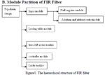
 

For anyone to help you, access to that paper is needed. Not everyone here is having IEEE login to view it.
 

Showing a block diagram won't be considered as copyright violation, I think.

As far as I understand, the paper is referring to parallel processing and distributed arithmetic, in so far it sounds unlikely that the implementation uses sequential circuits like state machines.
 
thanks . i didn't attached the paper because some times ago one of managers of forum told me that i shouldn't do it and that i should only provide the IEEE link . i attached some pics of the paper .can you tell me what is in the block diagrams ?

structure.png
 
Last edited by a moderator:

that's not the block diagram i meant ! i attached the block diagram that i meant here and the ROM address table too please don't delete them .
and i should ask a question about it to make it more clear :
our input is 8 bits but ROM address is 4 bits how should i connect them ?
**broken link removed****broken link removed**
 

i figured out how to implement shift register stage and ROM stage. but I'm stock at the tree shift adder stage . I implemented it from a block diagram from some other paper(i attached it ) and i attached my implementation too.
i have the following problems : 1-n stocks in 1 value and never changes .2- d should be 16 bits and ip1 and ip2 should be 32 bits but the multiplexer is supposed to put inputs directly into output according to sel. i tried to solve it by getting 16 bits of the inputs. is this way correct ?
11.png22.png
 

i altered my previous block diagrams to the one i attached and i got some output results that i don't know if its alright or not ! in the output waveform of my reference paper output stays zero for 7 rising edge of clock pulse and then it gets changed . for my design it changes after 2 . can anybody give me a hint ? am i doing right or not ? i checked every block on tree shift adder and the others blocks are fine but i don't have a clue what i should expect from the output.
new111.png
new result.png
 

Status
Not open for further replies.

Similar threads

Part and Inventory Search

Welcome to EDABoard.com

Sponsor

Back
Top