O
oneskeleton
Guest
Hey guys, I am having trouble solving a couple of homework exercises, I would really appreciate if you helped me understand the following exercises:
Exercise 1
Design a low frequency amplifier with two cascoding states, using the model with respective parameters: hie= 4 kΩ and hfe=200
First state: Voltage divisor resistance R1= 100kΩ , R2=10kΩ
Output resistance RC1= 10 kΩ
Second state:Voltage divisor resistance R1= 45kΩ , R2=5kΩ
Output resistance RC2= 3 kΩ
As for the input the signal source Vs with Rs=1kΩ is applied
Find AI,AIS,AV,AVS,Ri,Ro and Ro'
Exercise 2
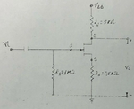
Design a low frequency FET amplifier considering Rd=5kΩ , Rs=0.5kΩ and Rg 1 MΩ. VDD applied is 30 V
Find the ID and gm values for the default configuration.
Find the voltage amplifier expression AVS
Hint: consider ID=16(1+VGS/4)2
This excercise is also accompanied by the attached image.
Please help me out if you can to understand how to solve these exercises quickly and sorry for the bad english, the exercises were translated from another language.
