Continue to Site

Welcome to EDAboard.com

Welcome to our site! EDAboard.com is an international Electronics Discussion Forum focused on EDA software, circuits, schematics, books, theory, papers, asic, pld, 8051, DSP, Network, RF, Analog Design, PCB, Service Manuals... and a whole lot more! To participate you need to register. Registration is free. Click here to register now.

[SOLVED] Power Factor using zero crossing

Status
Not open for further replies.

danielallucard

Newbie level 4
Joined
Jan 8, 2018
Messages
7
Helped
0
Reputation
0
Reaction score
0
Trophy points
1
Activity points
71
Dear all,


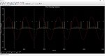
I'm trying to do a power factor measurement for academic work. I'm using the zero crossing detection on the voltage and the current so that I can do the difference between then and convert to angle.

Using the Op-Amp 741 as a voltage comparator I'm not able to get the phase wave of the current. It gives me the same result as the voltage.

I'm using a transformer in serie with the circuit as well as a current transformer but it gives no phase difference.

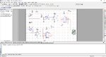
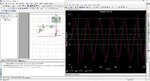
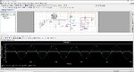
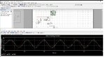
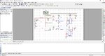
I'm attaching the printscreen of my circuit and my result as well.


Kind regards.
 

Attachments

  • Zero Crossing Voltage and Current.jpg
    Zero Crossing Voltage and Current.jpg
    395.3 KB · Views: 250
  • Result.jpg
    Result.jpg
    186.9 KB · Views: 179

Make sure T2 is a current xformer and has a burden resistor at the output.
Get rid of both diode bridges.
Output of the comparators to XOR gate.
 
Ok. I'll do it and post the results.
I'm going to see if I can find a current transformer on multisim because the only thing that I found was a Current Controller Source but I guess that is not the transformer.
I need to simulate a non invasive current transformer because in a factory we cannot open the circuit to meansure the current wave.
 

Rather than jump into this complicated schematic right away, try a basic approach. Read (a) the supply voltage waveform, and read (b) voltage waveform across R3. Compare them simultaneously. This ought to be a successful method to see several degrees of current lag in your setup. That is, power factor.

Add components to your bare schematic, one at a time. The 741 ought to have a dual supply, for the reason that the single supply results in its output staying above 2V, which is not reliable to appear as a 'low' to your 4093.
 
From the above pictures it is not clear the phase detected by the circuit output; the best approach would be superimposing the plot of the probe of both figures in the same graph, the current and voltage measurements. As suggested above, take the sample the analog values before plotting the digital result, so that it would be possible to know if at least the circuit is working as expected, whether it is measuring the phase correctly or not (for example, the model of a non-ideal transformer with parasitic inductance could add unwanted delay).
 

Last but not least;

On current transformers, the primary is the winding with the fewest turns (usually one) and the secondary is the one with many turns.
The CT should be labeled 1:10

Also, and AudioGuru would be very vocal about this, don't use a 741 as a voltage comparator. Use a proper device as the LM393 (dual) or a LM339 (quad).
 

Rather than jump into this complicated schematic right away, try a basic approach. Read (a) the supply voltage waveform, and read (b) voltage waveform across R3. Compare them simultaneously. This ought to be a successful method to see several degrees of current lag in your setup. That is, power factor.

Add components to your bare schematic, one at a time. The 741 ought to have a dual supply, for the reason that the single supply results in its output staying above 2V, which is not reliable to appear as a 'low' to your 4093.

Okay, I'll do a simple schematic just to meansure the voltage and the zero crossing at the voltage and post the results, after it I'll start to do the current meansure
 

I'm going to see if I can find a current transformer on multisim because the only thing that I found was a Current Controller Source but I guess that is not the transformer.
A current controlled current source models an ideal current xformer, so you can use it for the time being. Besides, how do you think the current xformer SPICE model looks inside ? ;-)
 
Rather than jump into this complicated schematic right away, try a basic approach. Read (a) the supply voltage waveform, and read (b) voltage waveform across R3. Compare them simultaneously. This ought to be a successful method to see several degrees of current lag in your setup. That is, power factor.

Add components to your bare schematic, one at a time. The 741 ought to have a dual supply, for the reason that the single supply results in its output staying above 2V, which is not reliable to appear as a 'low' to your 4093.

I have done it as two circuits, one more simple, just with an oscilloscope and a current clamp to see the phase between voltage and currend and gives me the result that is attached.

The Second one is a new zero crossing circuit. I changed the Op Amp to the LM 358 Dual Comparator and eliminated the diode bridge and add the voltage source to supply the IC.

Now the next step is to have the current wave so that I can see the time difference between them.

- - - Updated - - -

A current controlled current source models an ideal current xformer, so you can use it for the time being. Besides, how do you think the current xformer SPICE model looks inside ? ;-)

Good news,

I'm already been able to meansure the current wave using the current controller source.
I tried to insert the current controller source in the original circuit but I didn't have success.
If there is any advice please inform me.

Kind regards
 

Attachments

  • Wave forms.jpg
    Wave forms.jpg
    467.6 KB · Views: 153
  • Zero Crossing Tension.jpg
    Zero Crossing Tension.jpg
    355.9 KB · Views: 142
  • Zero Crossing Current.jpg
    Zero Crossing Current.jpg
    454.2 KB · Views: 159

As for the non-functional "Design 1" circuit with current transformer, the problem is that you didn't hear. It's been said that a current transformer must be operated with the lower winding side as primary and a shunt resistor on the secondary, so that the primary voltage drop is minimized.

The simulator doesn't complain, but a real OP would be destroyed by feeding +/- 25V to the input.

Sorry I didn't notice that I forgot to put a burden resistor.
I'm having trouble to model the current controlled current source because I have two CT's here that I want to model to multisim.
One is 30A/1V and the second one is 100A/50mA. The second one has a relation of 1:2000 and a burder resistor with 62 ohms.
The problem is that I cannot model it on the multisim.
 

Attachments

  • CT's.jpeg
    CT's.jpeg
    42.3 KB · Views: 113

Hi,

Why you can't model the CT?
* It's just one winding on the primary side and 2000 windings on the secondary.
* Use a meaningful coupling factor.
* use about 1:2000^2 in DC resistance ratio...with meaningful values
* use about 1:2000^2 in inductance ratio ... with meaningful values

For sure you know that your application
* can't work with low currents (did you consider to use a low_current_detection?)
* will work properly only with DC free sinusoidal currents (no rectifier load, no phase controlled load ...)

Klaus
 

Both CTs are 2000:1 current ratio, the "1V" types have a built-in burden resistor.

The problem is that I cannot model it on the multisim.
Means, you don't know how to describe a transformer in SPICE? An ideal linear transformer is modelled by coupled inductors with k=1, inductance ratio is the squared windings ratio. For 2000:1 current transformer e.g. Lprim = 100 µH, Lsec = 400 H
 
The other way around, I think.
No, just as written. 2000:1 current transformer has 1:2000 voltage ratio, respectively 1:2000² inductance ratio, as described by KlausST.
 
Finally I got the results that I wanted.

I completed the circuit using a simple trasformer as in the beginning but paying attention on the connection.
I put a tension divider after the potential transformer and a burden resistor as you all advised me.
After all the advices I finally finished the first part and the most important that is having the phase between both waves.
I have to use the schimmit trigger to convert the output signal of the LM358 to input in the microcontroller.

If there is any advices of how to improve the circuit is welcome.

PS: I had to put the burden resistor as 1K to see the current wave, but inside the CT that I have here is 62Ohms.

Kind Regards.
 

Attachments

  • Complete Circuit.jpg
    Complete Circuit.jpg
    394.5 KB · Views: 165
  • Simulation.jpg
    Simulation.jpg
    226.1 KB · Views: 116

If there is any advices of how to improve the circuit is welcome.
If you want the phase shift, take the outputs of the NAND gates or comparators and pass them to a XOR gate. Look at the output of the XOR gate.
 

Status
Not open for further replies.

Similar threads

Part and Inventory Search

Welcome to EDABoard.com

Sponsor

Back
Top