Continue to Site

Welcome to EDAboard.com

Welcome to our site! EDAboard.com is an international Electronics Discussion Forum focused on EDA software, circuits, schematics, books, theory, papers, asic, pld, 8051, DSP, Network, RF, Analog Design, PCB, Service Manuals... and a whole lot more! To participate you need to register. Registration is free. Click here to register now.

Flyback diode: it has one job, but mine sucks at it, why?

Status
Not open for further replies.
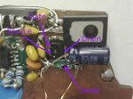
I'm still puzzled by what you are trying to achieve. It seems your circuit has no output and all you are doing is pulsing current through the coil then wondering why it shows a damped oscillation. The diode is connected directly across the coil and with the exception of it's turn-on time just clamps one polarity. Also note that the absolute maximum VDS of that MOSFET is 12V which you are exceeding. The layout is probably responsible for the 23MHz ringing, mounting the MOSFET on a small PCB and running wires to it is asking for trouble.

What drives the gate? We can't see the type when it is on it's edge. 820KHz is going to need quite a lot of gate drive power.

I also find it strange that a small air cored coil like that has 3 Ohms resistance - should be much less than that and almost certainly needs more inductance to be efficient.

Brian.

Brian,

Thank you for your comments. Allow me to try to explain as good as I can; I'm in this forum because I need your assistance, I'm lacking the valuable classical engineering training and the experience that comes along, therefore I would very much dislike to antagonize anyone here.

It seems your circuit has no output and all you are doing is pulsing current through the coil then wondering why it shows a damped oscillation.

You are right, I couldn't have expressed it more concisely myself. And I'm aware that makes me look like like I don't know what I want and why, but that is something I will have to live with because of two these two distinct reasons:

The first being embodied by the late Mr. Clarke, I'm paraphrasing here: "When a distinguished but elderly engineer states that something is possible, they are almost certainly right. When they state that something is impossible, they are very probably wrong."

The second reason being the Backfire Effect

So, - if you can fix the problem with the Backfire effect, I would be more than pleased to reduce any puzzlement that you may have.

maximum VDS of that MOSFET is 12V which you are exceeding.

Yes, I know, but it was never meant to exceed 6V, if that diode would just do as it is told ;-)

What drives the gate?

CMOS output into a B882/772 totempole, should be enough I believe.

The layout is probably responsible for the 23MHz ringing

I will change the layout and let you know the results. I note that CataM is also suggesting the same.

I also find it strange that a small air cored coil like that has 3 Ohms resistance

That is what I measure across the terminals. 0,05mm wire has about 0.5 Ohm per Meter.

should be much less than that and almost certainly needs more inductance to be efficient.

Can you please elaborate what you mean by "efficient" ? I'm not sure I understand?

- - - Updated - - -

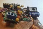
Move the inductor closer to the FET. You have big leads for the inductor, which likely are the reason for the 21.4 nH stray inductance. Inductor-FET-freewheeling diode --> All close together.

Thank you, out of sincere interest, can you please tell me how you deduct this causality?

- - - Updated - - -

Besides the dubious circuit purpose, it's quite difficult to read the experiment results. I don't see a single waveform with a clear description which voltage or current has been actually probed.

Can you please guide on how I should conduct the measurements so that they are clear, I mean - what did I miss?

- - - Updated - - -

Hello righteous,

The ringing is indeed caused by parasitic components associated with the physical realisation of this circuit, namely L and C that are not shown in the circuit schematic, but which exist in reality due to various factors. May I make 4 points that may help reduce the ringing effects, with reference to the sketch below (the quality of which I aplogise for, but a pencil and paper is all that I had).

1. Minimise the stray inductance contained in the loop enclosed by these three components: (a) the capacitor (b) the MOSFET (c) the diode. This is done by keeping component lead lengths short and minimizing the **area** of the circuit.

2. To reduce the parasitic L of the capacitor, connect a number of capacitors (of smaller value) in parallel rather than use one capacitor of larger value.

3. The length and the layout of the wires that connect the inductor to the circuit is not that important. The coil is already an inductor, so adding more parasitic L via longer wires is not going to contribute to the ringing. Use this fact to help acheive goals 1 and 2 above. The same can be said for the connection to the power supply, however if that voltage source is connected via significant parastic L then ensure there is plenty of C to "hold-up" the voltage of the loop mentioned in 1.

4. The connection of the gate driver to the MOSFET gate is important. In particular, the connection to the source terminal must be done as close to the component as possible to minimise including any L that carries the load current within the gate circuit. The gate drive should be low impedance, so standard circuit layout techniques should be applied such as (a) gate drive circuit to have good power suppy de-coupling capacitors, (b) small loop area from the de-coupling caps to the gate driver to the MOSFET (use twisted wires if necessary).

Even after all these actions have been applied, there still may be ringing, in which case standard snubbers (clamping type, and ramp-limiting type) may need to be applied, depending on what your final application is.

Hope this helps.

I just tried to load the image, but I am not sure it worked. If it did not, then I will try to load the image in my next post.

View attachment 143744

cascoder,

Thank you for your input.

Ad 1. Thank you again, its very clear from the drawing what you mean, I see it now.
Ad 2. Check - will do.
Ad 3. That seems to contradict the consensus here? Though my personal logic would be in line with yours "The coil is already an inductor, so adding more parasitic L via longer wires is not going to contribute to the ringing."
Ad 4. it's connected pin-to-pin, there is a total of 6mm of exposed wire in this connection.

Actually I think I will try to measure the inductance and let you know, I will be using this method
 
Last edited:
Thank you, out of sincere interest, can you please tell me how you deduct this causality?
Llumped,stray=1/(ω2·Coss@6V)=1/((2·Π·23.26 MHz)2·2190 pF)=21.4nH

Ad 3. That seems to contradict the consensus here? Though my personal logic would be in line with yours "The coil is already an inductor, so adding more parasitic L via longer wires is not going to contribute to the ringing."
I do not know why I thought you are connecting the diode directly across the inductor.. it is quite clear from your layout it is not like that... So, I agree with you.

- - - Updated - - -

Shows us the results with the improved layout when you are done. If you still have not acceptable oscillation and peak voltage, I think you need a RC snubber across the FET to damp those oscillations.
 

Llumped,stray=1/(ω2·Coss@6V)=1/((2·Π·23.26 MHz)2·2190 pF)=21.4nH

Thank you, is that a standard formula? Does it have a name? Where do you get the value for Coss from?

So if the stray is 21.4nH, what significance does this value have? what do you compare it against?

I do not know why I thought you are connecting the diode directly across the inductor.. it is quite clear from your layout it is not like that... So, I agree with you.

In the new layout the diode is now directly across the inductor.. what does that mean to the circuit performance?

Shows us the results with the improved layout when you are done. If you still have not acceptable oscillation and peak voltage, I think you need a RC snubber across the FET to damp those oscillations.

New layout
new-layout.jpg

And it can be seen that oscillations remain, but the peak voltage dropped to 14V now, which is good, but still not acceptable. So what is a good starting point for the RC values?
SDS00021.PNG

Closer look
SDS00020.PNG
 

In the new layout the diode is now directly across the inductor.. what does that mean to the circuit performance?
For me, directly across the inductor means it does NOT include the leads. So, do not do it. You had it O.K. how you used it, it was my fault for thinking that you have it that way.

Do this please: Connect the anode right as close as possible to the drain node and cathode right at the decoupling caps. This should include the leads of the inductor. Measure again what is the ringing frequnecy and what is its peak. Now that you have changed the layout, the stray inductance has changed.

Thank you, is that a standard formula? Does it have a name? Where do you get the value for Coss from?
It is the natural frequency of the oscillation of a series LCR circuit. In vulgar words, natural frequnecy is ~the oscillation frequency of the sinusoidal waveform.
Coss from datahseet of FET.

So if the stray is 21.4nH, what significance does this value have? what do you compare it against?
First, to see how bad your layout is and second for the RC snubber calculation.
 

Do this please: Connect the anode right as close as possible to the drain node and cathode right at the decoupling caps. This should include the leads of the inductor. Measure again what is the ringing frequnecy and what is its peak. Now that you have changed the layout, the stray inductance has changed.

Is this what you mean?
new-layout-closeup.jpg

The ringing frequency is now 38MHz
SDS00022.PNG
 

Yes. Now the peak is at about 7V, half from post #24. Is this acceptable for you ?

Yes and No, Yes because 7V would be workable, No because the peak shown is from the beginning of the trace since you only asked for frequency. here is another shot further along the time line, and the peak is 12 V. Snubber we welcome your dampening now ;-) You will note at this point the frequency is 3MHz lower than in the beginning.

SDS00023.PNG
 
Last edited:

Start with Csnubber=22nF and Rsnubber=1Ω
Expect >0.65 W power loss in the resistor.
 

Slowing the drain dV/dt by using a gate resistor or
gate resistor network could reduce the leading "kick".

But you also have to ask yourself whether this is a
problem, or just the ugly picture of the week. The
spikes may be an EMI issue or a transistor reliability
issue, or not, depending.
 

Start with Csnubber=22nF and Rsnubber=1Ω
Expect >0.65 W power loss in the resistor.

Thank you. I'll try it and let you know.

But >0.65 W power loss, isn't that quite a lot when there is already going 2-3A spikes through the diode?

- - - Updated - - -

Slowing the drain dV/dt by using a gate resistor or
gate resistor network could reduce the leading "kick".

But you also have to ask yourself whether this is a
problem, or just the ugly picture of the week. The
spikes may be an EMI issue or a transistor reliability
issue, or not, depending.

I will try with a gate resistor, I completely forgot about that.

But you also have to ask yourself whether this is a
problem, or just the ugly picture of the week. The
spikes may be an EMI issue or a transistor reliability
issue, or not, depending.

Or it could be the ugly picture of the week and a problem?

I would imagine that EMI is an issue, I mean theres a huge EMI generating device in the coil itself, would it do any good if I moved the coil further away from the semiconductors? And/or would it help if I made a 4 layer PCB all with SMD components, since the previous rearrangement of the layout after all made the spikes drop from 18-19V to 12-14V?

- - - Updated - - -

Start with Csnubber=22nF and Rsnubber=1Ω
Expect >0.65 W power loss in the resistor.

These are the results:

Peak voltage now at 11.5V

SDS00024.PNG

1. Moving the coil 150mm away from the semis reduced peak voltage with ~300mV, so I kept it like that time being.
2. Adding Csnubber=22nF and Rsnubber=1Ω reduced peak voltage with ~200mV, so I kept it like that time being.
3. Using a 1Ω gate resistor didn't do anything, but I kept it in anyway.
4. Using a 3Ω resistor instead of a coil, solved all problems, but the circuit was rendered useless, so I put the coil back ;-)
 

Start with Csnubber=22nF and Rsnubber=1Ω
Expect >0.65 W power loss in the resistor.

I had another coil lying around 500nH 6Ω so I tried that, and I got much cleaner switching (see below) and that got me thinking, what if I do it the other way around? I.e. adapting the inductor to the circuit? Which would be feasible as I got 0.15mm and 0.2mm wire and I have learned to measure the inductance, so why not.

The question is now, is there a way to calculate the induction so that I can have maximum current with least amount of ringing? (I know it's a trade-off like the snubber circuit) Otherwise I will just have to roll my own coils until I guesstimate it right.

500nH 6Ω coil, with snubber
with-snubber.png

500nH 6Ω coil, no snubber
without-snubber.png

500nH 6Ω coil, no snubber, ringing freq.
frq-no-snubber.png

- - - Updated - - -

I rolled another coil 3Ω 108nH, and that gives about 8V peak without snubber, and I got my current, so all in all it's acceptable (if I add the snubber).
 
Last edited:

I had another coil lying around 500nH 6Ω so I tried that, and I got much cleaner switching (see below) and that got me thinking, what if I do it the other way around? I.e. adapting the inductor to the circuit? Which would be feasible as I got 0.15mm and 0.2mm wire and I have learned to measure the inductance, so why not.
No. That is not the right way to do it. The not working snubber suggests that we need to estimate the parasitics better, experimientally, with the method I will show below.
I rolled another coil 3Ω 108nH, and that gives about 8V peak without snubber, and I got my current, so all in all it's acceptable (if I add the snubber).
So adding the snubber it works acceptable for you ? like the "500nH 6Ω coil, with snubber" ?

Estimation of parasitics experimentally:
1) In the original circuit (i.e. without snubber), using the coil you want and you want to snub, measure ringing frequency.
2) Add a capacitor between Drain and Source of the MOSFET with a value such that it reduces the ringing frequnecy substantially, e.g. until the new ringing frequency=original ringing frequnecy/2 (i.e. half of the original). To be half is just an example, it does not necessary need to make it to be half.. but change the original frequnecy substantially.
Note down the new ringing frequency and the capacitor you added in parallel that made that ringing frequnecy. The capacitor you added between Drain and Source of MOSFET call it Cadded.
3) Definition: ratio=foriginal ringing/fnew ringing
4) Cparasitic,experimental=Cadded/(ratio2-1)
5) Llumped,stray,experimental=1/((2·Π·foriginal ringing)2·Cparasitic,experimental)
 

    V

    Points: 2
    Helpful Answer Positive Rating
So adding the snubber it works acceptable for you ? like the "500nH 6Ω coil, with snubber" ?

Well I mean the "500nH 6Ω coil, with snubber" wave form would be acceptable, but I would like it with the 108nH/3Ω coil which is more suitable for the purpose. It seems there is not many further options than the snubber. Now I will try to do the estimation of parasitics experimentally and revert accordingly.
 
Last edited:

All diodes have a finite "turn on" time, the faster they turn off the slower they turn on, the volts overshoot while the diode is becoming fully saturated in the forward direction (all charge injection to the depletion region has occured) - large shottkies perform better at turn on in this regard (but have more intrinsic capacitance at diode turn off) so once the loop inductance of the turn off circuit has been removed you are stuck with the diode properties, and MBR10100 will show you this, largish snubbers across the diode will help reduce the forward overshoot too. Welcome to power electronics design...! where even the apparently simple things are complex.

p.s. @ betwixt, this type of ckt is used a lot to drive relays at a lower but sustained current to reduce their dissipation at high ambient, the ckt used usually provides 12V (or whatever) for 0.5sec then PWM reduced to ~75% current...

- - - Updated - - -

Too long a gnd lead on your scope probe can give you overshoot "appearance" when there is none or very little, wrap the gnd led around your probe tip as many times as it will go and find a gnd close to the point you wish to measure - if there is a difference then this is part of the problem ...
 

Estimation of parasitics experimentally:
1) In the original circuit (i.e. without snubber), using the coil you want and you want to snub, measure ringing frequency.
2) Add a capacitor between Drain and Source of the MOSFET with a value such that it reduces the ringing frequnecy substantially, e.g. until the new ringing frequency=original ringing frequnecy/2 (i.e. half of the original). To be half is just an example, it does not necessary need to make it to be half.. but change the original frequnecy substantially.
Note down the new ringing frequency and the capacitor you added in parallel that made that ringing frequnecy. The capacitor you added between Drain and Source of MOSFET call it Cadded.
3) Definition: ratio=foriginal ringing/fnew ringing
4) Cparasitic,experimental=Cadded/(ratio2-1)
5) Llumped,stray,experimental=1/((2·Π·foriginal ringing)2·Cparasitic,experimental)

I did the experimental procedure, so what do I do now with the calculated value?

ad. 3 Ratio=foriginal ringing/fnew ringing=37MHz/23MHz=1.6

ad. 4 Cparasitic,experimental=Cadded/(ratio2-1)=4.7nF/(1.62-1)=3nH

ad. 5 Llumped,stray,experimental=1/((2·Π·foriginal ringing)2·Cparasitic,experimental)=1/(2·Π·37MHz)2·3nH=6nH

Here's the scope shot, the blue is the foriginal ringing and yellow is fnew ringing
parasitic-1.png

- - - Updated - - -

Welcome to power electronics design...! where even the apparently simple things are complex.

First of all thank you for you warm welcome, I enjoy it very much here, I feel much closer to mother nature than I did with digital which is very confined.

All diodes have a finite "turn on" time, the faster they turn off the slower they turn on, the volts overshoot while the diode is becoming fully saturated in the forward direction

Yes I'm aware of that, but due to my limited experience I thought; If I pick a diode with fast turn on time, then turn off time would follow proportionally. the PMEG2020 I have chosen is rated at 20V, 2 A(continuous) 5A(peak) 450 mV voltage drop, 5 ns turn on time. The MBR10100 and the SB220(which I have in my stash) have turn on times that are not even worth mentioning in the datasheet, I'm guessing it's a few hundred nano seconds. That's why I chose PMEG2020, but is that a wrong choice you say? Should I go big and sluggish?

And thanks for the scope probe tip ;-)
 

Hi,

I did not go through the whole thread...


But just looking at the last scope picture.
Blue = original waveform
Yellow = new waveform

I see the damping ratio is less than before, and frequency is less than before.
This tells me that your damping circuit is too low impedance (referenced to ringing source impedance)....most if the energy is stored in the capacitor instead of being dissipated in the resistor.

You can measure the voltage across the resistor....
I assume increasing the resistor value to 10 Ohms or even 100 Ohms will increase the damping ratio.

The best damping ratio will be when the resistor value is in the range of the source impedance value.

After choosing the correct resistor value you may also reduce the capacitor value. This decreases overall power dissipation and thus increases efficiency.

This is just an assumption. I did not calculate through your circuit.

Klaus
 

Now design the RC snubber as we did before.
Parasitics did not change much regarding the Coss@6Vds~2.2 nF.

Rsnubber=1/(2·ξ) · √(Llumped,stray,experimental/Cparasitic,experimental) = 0.7Ω so you can use 1Ω as before. ξ=1 because we want high damping.
Csnubber=22 nF as before.

If this values do not help, play with Csnubber by increasing it... However then the power loss increases.
If that does not help either, play with Rsnubber by decreasing it.
Also keep in mind that you must fulfill this inequality: 3·Rsnubber·Csnubber << On time of the MOSFET

If that does not help either, try with Csnubber=4.7nF and Rsnubber not changed (~0.7Ω). However, I have next to no expectations that this low value of snubber cap would work.

- - - Updated - - -

After choosing the correct resistor value you may also reduce the capacitor value. This decreases overall power dissipation and thus increases efficiency.
Agreed.
 
Last edited:

Hi,

I did not go through the whole thread...


But just looking at the last scope picture.
Blue = original waveform
Yellow = new waveform

I see the damping ratio is less than before, and frequency is less than before.
This tells me that your damping circuit is too low impedance (referenced to ringing source impedance)....most if the energy is stored in the capacitor instead of being dissipated in the resistor.

You can measure the voltage across the resistor....
I assume increasing the resistor value to 10 Ohms or even 100 Ohms will increase the damping ratio.

The best damping ratio will be when the resistor value is in the range of the source impedance value.

After choosing the correct resistor value you may also reduce the capacitor value. This decreases overall power dissipation and thus increases efficiency.

This is just an assumption. I did not calculate through your circuit.

Klaus

Thank you for your suggestion. The reason for capacitor only is that Mr. CataM is trying to give me a lesson in the exquisite procedure for correctly dimensioning a snubber ref. post #33
 

Looking at your blue trace it is not too bad, a small snubber should compensate, smaller C (x 0.3 or smaller, and similar or larger R)

- - - Updated - - -

If you go to 5x the junction capacitance (~ 50pF) then a 330pF or 470pF cap should be heaps and you will have to experiment to find the correct R value (100 ohms starting..?) 0805 or 1206 directly across the diode. X7R dielectric as a minimum, preferably C0G (NPO).

A snubber across the driving fet can be of benefit too.

The power in the snubber R will be V^2 C Freq so for 10V, 100kHz, 470pF ~ 47mW, 10MHz = 470mW.
 

Status
Not open for further replies.

Similar threads

Part and Inventory Search

Welcome to EDABoard.com

Sponsor

Back
Top