Continue to Site

Welcome to EDAboard.com

Welcome to our site! EDAboard.com is an international Electronics Discussion Forum focused on EDA software, circuits, schematics, books, theory, papers, asic, pld, 8051, DSP, Network, RF, Analog Design, PCB, Service Manuals... and a whole lot more! To participate you need to register. Registration is free. Click here to register now.

Need help on HFSS simulation of IFA antenna

Status
Not open for further replies.

SuBill

Junior Member level 3
Joined
Oct 4, 2017
Messages
27
Helped
0
Reputation
0
Reaction score
0
Trophy points
1
Activity points
308
Dear all,

I'm new of RF design, especially HFSS simulation. I'm so confused of how to really design and simulate an antenna correctly using HFSS. Please help me in these following regards:

1. Lumped port position:
- I know it should be between the ground plane and the signal path. But for an IFA as attached (designed by TI, for 900Mhz), I'm not sure where to put the port. The pink one is the lumped port. Is it correct?
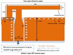
- For the more complicated IFA antenna (2nd file attached), where should I put the port? Is it between the end of the antenna trace (right at the text "50ohm transmission line" and the bottom layer which acts the RF ground plane? If yes, in details, I'll draw a port at the end of the trace going down to the bottom layer?

2. Virtual radiation boundary and air box:
- The correct virtual radiation boundary dimension should be more than lamda/2, right? Can I just simply make the distance from each edge of the substrate to any face of the boundary to be slightly more than lamda/4?
- The air box is made 30% bigger than the virtual radiation boundary.

4. Design parameters:
- Could you please give me any equation or method to design an IFA antenna? I've read some materials and they just gave out the parameters, not how to do it. So when I got problem with the result, I do not know how to adjust them.
- For the IFA designed by TI, if I put a bottom layer as another GND plane, the simulated result was totally wrong!

Thank you very much and look forward to your support!
IFA_TI.jpg
IFA_Cypress.jpg
 

I'm not an HFSS user, so this is more generic without the actual terms used in HFSS.

I'm not sure where to put the port. The pink one is the lumped port. Is it correct?

Lumped ports give best results if port length is much smaller than wavelength. Long ports will introduce parasitics due to their size, e.g. series inductance. So here, the pink line should be a line (conductor) with a small lumped port at the end.

Is it between the end of the antenna trace (right at the text "50ohm transmission line" and the bottom layer which acts the RF ground plane? If yes, in details, I'll draw a port at the end of the trace going down to the bottom layer?

Yes, both is correct.

For the IFA designed by TI, if I put a bottom layer as another GND plane, the simulated result was totally wrong!

Yes, there must be NO ground under the radiator. Bottom ground is only in that area where you see top ground also.

For the other questions, I don't know.
 

I'm not an HFSS user, so this is more generic without the actual terms used in HFSS.


Lumped ports give best results if port length is much smaller than wavelength. Long ports will introduce parasitics due to their size, e.g. series inductance. So here, the pink line should be a line (conductor) with a small lumped port at the end.


Yes, both is correct.


Yes, there must be NO ground under the radiator. Bottom ground is only in that area where you see top ground also.

For the other questions, I don't know.

@SLK001: Thank you for your comment, but I have to know sth about antenna design. So I'm learning now.

@volker@muehlhaus: Thank you so much for your clear explanation about the lumped port. Now I understand more.

For ground of the 2nd IFA antenna (designed by Cypress), is the top ground connected to the bottom ground through drill vias? As I've read from one PIFA article (Iulian Rosu, YO3DAC / VA3IUL), I understand that drill vias are the method to increase the bandwidth. So if I'm okay of narrower bandwidth, can I just lay the bottom GND there without any drill via? If I do so, there will be 2 GNDs in my circuit. One is, say, antenna GND, and the other can be the analog GND for ICs. Is it okay to do this?

In HFSS simulation, the result has changed when I expanded the dimensions of virtual radiation box and air box. In my case (TI design) it was worse. I'm still wondering which dimension is correct.
 

If I do so, there will be 2 GNDs in my circuit. One is, say, antenna GND, and the other can be the analog GND for ICs. Is it okay to do this?

No.

How can current flow between unconnected grounds? GND is what you use for current return. No connection, no current flow.
 

No.

How can current flow between unconnected grounds? GND is what you use for current return. No connection, no current flow.

Yes, you're so right. Thank you very much for your quick response :)
 

- The correct virtual radiation boundary dimension should be more than lamda/2, right? Can I just simply make the distance from each edge of the substrate to any face of the boundary to be slightly more than lamda/4?

Radiation boundaries can typically be up to lambda/4 distance from any conductor. Generally, the further away they are, the better, but this causes your simulation to be larger.

- The air box is made 30% bigger than the virtual radiation boundary.

Typically the radiation boundary is placed on the air box. What have you placed it on?
 

Radiation boundaries can typically be up to lambda/4 distance from any conductor. Generally, the further away they are, the better, but this causes your simulation to be larger.


Typically the radiation boundary is placed on the air box. What have you placed it on?

@ PlanarMetamaterials: Thank you for your response. In an antenna example design by HFSS Design Kit (for example a dipole one), there are two boxes. One is called virtual radiation box which was explained to model the practical environment (?) around the antenna. The other one is the air box which is assigned radiation boundary (radiating only, in this case). The air box is larger than the virtual box. So for my antenna design, I followed these models and made 2 similar boxes.

I'm also wondering whether I should select different radiation boundary other than "Radiating only" for a receiving antenna. Have you guys simulated a receiving antenna and which differences should I make/select for it?
 

Status
Not open for further replies.

Part and Inventory Search

Welcome to EDABoard.com

Sponsor

Back
Top