Continue to Site

Welcome to EDAboard.com

Welcome to our site! EDAboard.com is an international Electronics Discussion Forum focused on EDA software, circuits, schematics, books, theory, papers, asic, pld, 8051, DSP, Network, RF, Analog Design, PCB, Service Manuals... and a whole lot more! To participate you need to register. Registration is free. Click here to register now.

Fully Differential Opamp Simulation with Switched Capacitor CMFB

Status
Not open for further replies.

Puppet123

Full Member level 6
Joined
Apr 26, 2017
Messages
356
Helped
22
Reputation
44
Reaction score
21
Trophy points
18
Activity points
3,059
dopamp.pngdopamp.png

Hello,

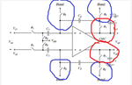
I am attempting to simulate this Fully Diffferential Opamp with SC CMFB.

I need to get the SNDR to 70dB.

Should I use Transmission Gates for the Switches shown in the figure below ? What strategies can I use to increase the SNDR ?

Thank you in advance for advice and tips.
 

Last edited:

Hello erikl,

Thank you for your response.

I have a few questions:

1. Why not use all transmission gate switches ?

The paper you refer to states on page 3:

"It is worth noting that the 0.5-b redundancy is obtained using only two non-overlapping phases (phase1-phase2) and the complementary ones (since all the switches are implemented as transmission gates)."

2. What do you mean by NMOS switches with a second anti-phase switched NMOS Cap ? What is an anti-phase switched NMOS cap ? Sorry for my ignorance on this topic.

3. So when you say PMOS switches you just mean PMOS switches by themselves, obviously. Again, I apologize for my ignorance on these topics.

Thank you for your assistance!
 

1. Why not use all transmission gate switches ?
This depends on the potential (voltage levels) between the nodes you want to switch:

If you need to switch a short circuit between nodes of nearly the same potential - like M14, M15 & M16 in Fig.4 of my above cited paper - a single MOS should be enough. It's polarity doesn't really matter, you can use an NMOS or a PMOS. Depends much more on the convenient accessibility of the corresponding clock phase in layout.

In case you want to switch a positive potential node to GND, an NMOS is the right choice, cf. M12, M13 of Fig.4 . A negative potential compared to VDD of course should be switched by a PMOS, s. M10 & M11 in this fig.

If the potential to be switched - compared to the reference of the switch - is unknown, i.e. could be positive or negative, a transmission gate should be used, like all the switches in Fig.2 & 3 of the paper.


2. What do you mean by NMOS switches with a second anti-phase switched NMOS Cap ? What is an anti-phase switched NMOS cap ? Sorry for my ignorance on this topic.
See here: minimize_charge-injection.png Find here an explanation.

3. So when you say PMOS switches you just mean PMOS switches by themselves, obviously.
Right!
 

Ok, thank you for your answer.

But for the figure that I posted, should all transmission gates be used then ?

What I did was use transmission gates for all the switches used and did not get the 70dB SNR I needed and instead got half of that - 35 dB SNR.

According to your reasoning, as I interpret it, I should use all transmission gates since I am not sure about the voltages at the nodes.

Sorry if I misunderstood. Thank you for your help.
 

Hi,
If you think the switches are the problem, a simple switch won't do the work. That's because the Vgs of the switch varies with the input voltage. This means that the on resistance varies. I think you might need a circuit to make the Vgs of the switch constant. But this will affect the SNDR not the SNR. If the SNR is the problem, you need to work on the noise of the circuit.
 

... for the figure that I posted, should all transmission gates be used then?

According to your reasoning, as I interpret it, I should use all transmission gates since I am not sure about the voltages at the nodes.

Right: all switches external to the diffAmp should be transmission gates:

Puppet123_SC_diff-amp.png
 

Erikl,

Thank you for your response.

How about the switches internal to the diff amp, they are not tranmission gates right.

Just used NMOS tranmission gates or do I use PMOS ?

Thank you again.
 

Zooner,

Thank you for your response.

Yes, the SNDR is the problem.

Are you suggesting I use a bootstrapped switch then. If I use the bootstrapped switch, then since the circuit is differential do I apply that switch to all switches ?

Thank you.

- - - Updated - - -

Erikl,

Thanks for your message.

Re-reading your post they should all be transmission gates even internally to the diff-amp, since the voltages between the switches are unknown.

My apologies, as I am new to this topic, thank you for your patience.
 

Erikl,
Re-reading your post they should all be transmission gates even internally to the diff-amp, since the voltages between the switches are unknown.

No! Seems you misunderstood me:

Fig.4._Fully_differential_Switched_Opamp.png

The voltages between the switches are known, simple MOS switches are sufficient (M10..M16).
 

Erikl,

Thank you again for your response.

I marked up my original attachment - so I am sure the ones I circled in blue can be NMOS switches, and somewhat sure the ones in red can also be NMOS switches.

Is this where I should add the NMOS switches with a second anti-phase switched NMOS Cap as you had previously suggested as well ?

Thank you again for your patience and understanding as I am new to this area.

- - - Updated - - -

@Zooner and @Erikl,

Just so I understand correctly, in order to achieve 70dB SNDR from this configuration, I must optimize both the opamp noise and also the switch configuration in order to achieve the desired SNDR - and minimize both noise and distoration.

Is this thinking correct ?

Thank you.
 

Attachments

  • dopamp_markedup.png
    dopamp_markedup.png
    20.3 KB · Views: 390

I marked up my original attachment - so I am sure the ones I circled in blue can be NMOS switches, and somewhat sure the ones in red can also be NMOS switches.
https://www.edaboard.com/attachment.php?attachmentid=144026&d=1516237430
These switches are external to the diff amp! Node voltages to be switched are unknown - here you need transmission gates!


Is this where I should add the NMOS switches with a second anti-phase switched NMOS Cap as you had previously suggested as well ?
In order to reduce charge injection, you should add a second anti-phase switched MOS Cap in series with each proper switch, i.e. for transmission gates, too.
 

Hi,
Yes, if you want the required SNR, SNDR you need to work on noise and on switches. I don't think you need boostrapped switches everywhere. You need them in places where you see that the VGS of a normal switch varies a lot (because this is what makes the on resistance nonlinear).
 

@Zooner, thanks for your response.

How would I check to see whether the VGS of the normal switch varies a lot - would that usually be at the input - like at the VS1 and VS2 of my attached fully differential opamp ? I attached it again - so maybe bootstrapped switches at points not in blue or red - Also around maybe the VBB - those switches ?

Or does one check all the nodes in the circuit or is there a general rule of thumb?

Thank you again.
 

Attachments

  • dopamp_markedup.png
    dopamp_markedup.png
    20.3 KB · Views: 165

Hi,
I think the red switches, and the two input switches should be boostrapped, since they are in the signal path. The rest can be simple switches.
 

@Zooner, thank you for your reply.

By simple, do you mean transmission gates or nmos switches - I assume transmission gates.

Thank you.
 

Status
Not open for further replies.

Part and Inventory Search

Welcome to EDABoard.com

Sponsor

Back
Top