Continue to Site

Welcome to EDAboard.com

Welcome to our site! EDAboard.com is an international Electronics Discussion Forum focused on EDA software, circuits, schematics, books, theory, papers, asic, pld, 8051, DSP, Network, RF, Analog Design, PCB, Service Manuals... and a whole lot more! To participate you need to register. Registration is free. Click here to register now.

Current mirror layout with odd multiplier

Status
Not open for further replies.

sthota04

Newbie level 5
Joined
Oct 26, 2015
Messages
9
Helped
0
Reputation
0
Reaction score
0
Trophy points
1
Activity points
67
Please have a look at the current mirror below.

I Call the diode connected transistor as A and the transistor in which the current is being mirrored as B.
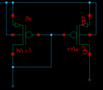
Capture.PNG

If A (m=1) and B (m=3), How should I place the devices. I can only see the following possibilities.

Dummy,B,B,A,B,Dummy

or

Dummy,B,A,B,B,Dummy

But I still suspect there would be linear gradients with the above two arrangements.

Please give me your suggestions to tackle this.
 

Use an extra B device which is not connected:
Dummy,B,B,A,B,B,Dummy
 

Or make it 2:6

DBBABBABBD or DBBBAABBBD or DABBBBBBAD

If they're wide enough that 2 fingers per leg makes
sense
 
Or make it 2:6

DBBABBABBD or DBBBAABBBD or DABBBBBBAD

If they're wide enough that 2 fingers per leg makes
sense

Which of the above two arrangements are preferred and why?
 

That, I couldn't tell you. All are center-symmetric. I
kind of like the first one as the reference devices
are most evenly distributed in the rack. But science,
I have none.
 
D,B,B,A,B,D
D,B,A,B,B,D

So many options...
 

Status
Not open for further replies.

Similar threads

Part and Inventory Search

Welcome to EDABoard.com

Sponsor

Back
Top