Continue to Site

Welcome to EDAboard.com

Welcome to our site! EDAboard.com is an international Electronics Discussion Forum focused on EDA software, circuits, schematics, books, theory, papers, asic, pld, 8051, DSP, Network, RF, Analog Design, PCB, Service Manuals... and a whole lot more! To participate you need to register. Registration is free. Click here to register now.

Operational trans conductance amplifier working

Status
Not open for further replies.

ICdesignerbeginner

Member level 5
Joined
Nov 22, 2017
Messages
86
Helped
1
Reputation
4
Reaction score
2
Trophy points
8
Activity points
729
Hi

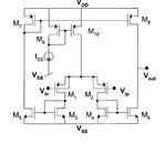
Can some one help me in understanding this OTA confguration. I have seen different OTA configuration but this OTA configuration attached below has three current mirrors to pass the current to the output. What about the ac current? I think current mirrors work for DC currents then how will ac current appear at output?
OTA.jpg
 

thank you for your reply.

can you please help me in understanding If all the three current mirror currents are same then it means the output current will be zero? AC and DC both?
 

If all the three current mirror currents are same then it means the output current will be zero? AC and DC both?

Why zero? The DC current injected by the DC current source ISS is copied (possibly multiplied) via M9 to M10, one half of this current is copied by the mirror M3->M5 to the mirror M7->M8, the other half via the mirror M4->M6. This results in a DC current equal to one half of the current through M10 (if no current multiplication by the mirrors has to be considered).

Injected ac currents by the impedances of M1 & M2 - amplified by the OTA transistors M1 .. M4 - will equally be mirrored via M3->M5->M7->M8, as well as M4->M6, where the ac output voltage vout is generated via the transimpedances of M6 & M8 . The ac OTA currents through M1-M3 and M2-M4 are anti-phase, so they will be added.

DC currents generated (copied) by mirrors are reproduced as absolute (fixed) values, hence will not be added by such mirror circuits - there's no anti-phase current generation as by the OTA transistors M1 .. M4 (DC currents have the same direction).
 
Thank you erikl for your detailed reply. I understand all your described working of OTA but I was saying about output zero for DC because let suppose I have 10u amp ISS and 5u A passing through M1 and M3, similarly 5u A passing through M2 and M4 the same 5uA current is copied from M3 and M5 - M7 to M8. It means 5uA current is flowing through the drain of M8. Similarly 5uA is flowing through M4 to M6. It means 5uA is flowing through the drain of M6. Now if 5uA flowing through M8 is flowing down to M6 then it means no current is flowing out of the OTA. then DC current is zero.

This type of current mirrors are class AB structures. Am I right?
 

This type of current mirrors are class AB structures. Am I right?
Class AB or class B are classifications for bipolar amplifier output stages and not applicable to unipolar current sources.

The OTA signal path is actually implemented as pure class A.
 

... Now if 5uA flowing through M8 is flowing down to M6 then it means no current is flowing out of the OTA. then DC current is zero.

This is correct if you have only a capacitive load (e.g. CMOS gate(s)). A resistive load would of course draw an appropriate DC current, which, by this, would change the output operation point voltage.
 

inverting current.jpg

I have attached a schematic. M17-M20 are invertig the current how is it inverting. Is it inverting the ac current? or Dc? M12, M14, M15 and M16 is producing positive current io+ and M17-M20 is producing negative current io-. I cant underatnd how is this happening. The current comming from the load transistors ar now coming from the source transistors thats why? or is there any other reason?
 

M17-M20 are invertig the current how is it inverting.
They don't invert.

Is it inverting the ac current?
No, not the transistors. The ac current "inversion" is evoked by feeding a (e.g.) VDD-referenced ac current from the upper PMOS to the lower NMOS, where this very same ac current gets GND-referenced, which causes the "inversion" (same current, but now referenced to the opposite terminal).

No, if you think of absolute value, or current direction. Of course you could say: VDD via the PMOS sources the current, and the NMOS sinks the current to GND. If you refer this (same) current to its associated terminal, so it's sourced by VDD and sunk by GND, which you also might consider as inversion, like in the ac case.

M12, M14, M15 and M16 is producing positive current io+ and M17-M20 is producing negative current io-
Here, we must differentiate between the DC & the ac path:

The mirror master M11 from the left Vi- branch reproduces its both DC & ac currents (possibly multiplied by the ratio of the W/L ratios of the involved MOSFETs) by mirror slave M12, which feeds these currents to NMOS mirror master M15, which - on its part - feeds this same current to NMOS mirror slave M16. The PMOS mirror master M13 from the right Vi+ branch via the PMOS mirror slave M14 closes this DC path.

The ac current part from the left Vi- branch (let's call it i-) via M11 & M12-M15-M16 arrives inverted (GND-referenced) as -i- at node Io1, whereas the ac current part from the right Vi+ branch (i+) - which is inverted itself compared to the left part - arrives via M13-M14 non-inverted as i+ at node Io1, where they get added:
-i- + i+ = i+ - i- = 2i+ (as i- = -i+).

Similar argumentation applies to the Io2 node.

The current comming from the load transistors ar now coming from the source transistors thats why?
It's the same current, s. above!
 

Status
Not open for further replies.

Similar threads

Part and Inventory Search

Welcome to EDABoard.com

Sponsor

Back
Top