Continue to Site

Welcome to EDAboard.com

Welcome to our site! EDAboard.com is an international Electronics Discussion Forum focused on EDA software, circuits, schematics, books, theory, papers, asic, pld, 8051, DSP, Network, RF, Analog Design, PCB, Service Manuals... and a whole lot more! To participate you need to register. Registration is free. Click here to register now.

How to make an fast Analog Switch?

Status
Not open for further replies.

righteous

Full Member level 2
Joined
Nov 29, 2017
Messages
130
Helped
0
Reputation
0
Reaction score
0
Trophy points
16
Activity points
1,282
Dear Engineers (both pro and amateurs),

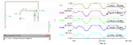
I would be grateful if someone could throw me a bone here, a general idea of the direction would suffice, on how to make a fast analog switch that will do the following:

Screenshot from 2017-12-20 14-22-29.png

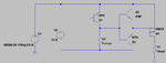
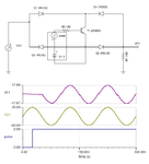
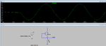
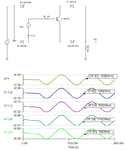
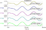
My challenge is to make an analog switch that is open during the first positive (half) period of PULSE. I'm personally thinking along the lines of a thyristor here...

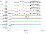
I don't know much about the voltage source at this point, but it can also source current, 20-40mA would be a good guesstimate, and I would like to pass both voltage and current through the switch.

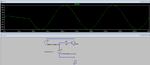
BTW: I also have access to the timing signal (both INV and non-INV) that triggers the pulse, it's a CMOS output and is aprox. 100ns wide.
 
Last edited:

Thyristors are slooooooooooooooow switchers. Use a Mosfet.
 

Incomplete specification, many unclear details.

I understand so far:

You want to pass one positive half wave through the switch (50 ns width) and cut negative and succeeding half waves.

Load impedance is in the kOhm range.

How about acceptable switch voltage drop, waveform distortion, isolation in off state?

Thyristor is surely inappropriate due to recovery time in the 10 µs range.
 

Dear FvM,

Incomplete specification, many unclear details.

I do appreciate that engineers like full specs and clear constraints, however I don't like to start with constraining my self when I don't know which direction to go, so everything is very flexible at this point, please bear with me I'm an artist, much like this French dude:
France-01.jpg


You want to pass one positive half wave through the switch (50 ns width) and cut negative and succeeding half waves.

Well, almost - I want to pass one positive half wave through the load resistor, and pass the succeeding positive and negative half-waves through the switch, the schematic may not reflect my intention as good as I thought.

Load impedance is in the kOhm range.
At the time of writing, I still don't know how the rest of the circuitry after the switch should look like, it depends what can be done with the switch.

How about acceptable switch voltage drop, waveform distortion, isolation in off state?

Obviously as ideal as possible, but it depends.... I mean sometimes you can sacrifice speed for performance and vice versa, it all depends on the initial direction, for which I'm asking assistance.

Thyristor is surely inappropriate due to recovery time in the 10 µs range.

Then FET it is as Mr. Schmitt indicates. But how to switch a FET in AC? How do you maintain a Vgs(ON) in AC conditions?
 

At the time of writing, I still don't know how the rest of the circuitry after the switch should look like, it depends what can be done with the switch.
I think in general things are done the other way around. You set the objective and then find solutions to achieve the objective. The switch and its corresponding driving circuitry are the last thing to do, after all specs involving the switch are laid down.
 
Last edited:

I think in general things are done the other way around. You set the objective and then find solutions to achieve the objective. The switch and its corresponding driving circuitry are the last thing to do, after all specs involving the switch are laid down.

As I said, I appreciate that it is the normal way of doing things in electronic engineering. That is why I requested the good engineers to please bear with me. I obviously have a very good reasons for why I'm working like I do.

- - - Updated - - -

One simple solution could be a peak detector with its signal conditioning to drive the FET. Another more involved one could be a charge pump derived from your sinusoidal source and additional comparators... It all depends on what do you have available.. but since your post #1 is so little on details, we can just throw unnecessary staff out there. .

First of all I have nothing available except basic components, scope, soldering iron and an account with Farnell, so it doesn't really matter what I have available, I have to source it first.

Secondly I'm intrigued that the absence of constraints is perceived as an constraint, whereas I personally think it's the better not to have constraints. It's not like I request a complete production ready solution, just a hint to get me in the right direction, and only then I can come up with more details and constraints.

I Found this on the ol' interwebs, would this be a viable solution?

YZVOX.gif

Obviously I can't use opto coupler, they are too slow.
 

Hi,

"access to the timing signal (both INV and non-INV) that triggers the pulse, it's a CMOS output and is aprox. 100ns wide"

Maybe a dual comparator, each of the comparators with opposite trigger levels, one to sink the current in the resistor and the other to turn on/off the MOSFET switch. If the signal is 40V then I suppose you would need a resistor voltage divider to lower the input voltage to the comparators.

Also, if that could work, I guess you may need a separate power supply for whatever you use to sense positive and negative half and trigger the switch. For example, I don't know of any comparators that work over about 30V supply or near that for the inputs, the output is different.

Another way to go could be an op amp based polarity detector circuit, not sure about such a fast op amp, 'though, high speed usually involves increased cost, and you seem to need something very fast. Again, the vague description seems to lead to the conclusion that a separate power supply will be needed for the polarity detection and control circuitry.
 

First of all I have nothing available except basic components, scope, soldering iron and an account with Farnell, so it doesn't really matter what I have available, I have to source it first.
Asking if you have available something does not mean you need to have it right away, but if you are not constrained by that (e.g. because of money, size etc..).
I Found this on the ol' interwebs, would this be a viable solution?
From the description you provided in post #4, you need a 2 quadrant switch, which is achievable with a single N-MOSFET having its source connected to the input. The low performance of the diode can be bypassed by using the MOSFET when required.
The switch realization you are showing achieves the intended operation too. So, to answer your question, yes, it is another possibility, which has additional unnecessary MOSFET.
 
Last edited:

100nS period is not especially fast. The 40V however
puts you in very slow technologies. It's spec-marginal
(or over the top) for the "40V" (36V) analog switches
generally.

Prop delay for such IC switches can be expected to be
over 100nS.

At such low currents, and only caring about the negative
cycle, a PJFET switch could be practical (depending on
what the "to" node is doing - for example a PJFET used
to allow, or not, current to a summing virtual ground
node would be a happy choice, but if "to" has to follow
"from" across a range of voltage (as an ideal general
purpose switch must) then the gate drive would be a
mess (done that, PJFET switches and muxes in 40V
BiFET technology).

In the switch-to-virtual-ground case the gate drive
is bone simple (you could use a CMOS gate 0-xV as
long as X exceeds VPO).

So one input for you is, be clear about "how switchy
is my switch"? True general-purpose-ness almost
always means heavier lifting and fewer choices of
platform, than a tailored switching circuit where
things that aren't needed, are disregarded. The
questions about the bigger picture go to this point.
 

Asking if you have available something does not mean you need to have it right away, but if you are not constrained by that (e.g. because of money, size etc..).

I understand. Obviously I'm constrained like every other poor man, but allow me to quote Teddy Bass "Where there's a will - and there is a f****** will - there's a way - and there is a f****** way "

From the description you provided in post #4, you need a 2 quadrant switch, which is achievable with a single N-MOSFET having its source connected to the input. The low performance of the diode can be bypassed by using the MOSFET when required.

Now that's a good idea! but that would require the diode to be slower than the width of the first half-period? And how do you maintain the Vgs when source is fluctuating 40 Vpp? The latter would be my biggest conundrum due to my lack of analog experience.
 

At such low currents, and only caring about the negative
cycle, a PJFET switch could be practical (depending on
what the "to" node is doing - for example a PJFET used
to allow, or not, current to a summing virtual ground
node would be a happy choice, but if "to" has to follow
"from" across a range of voltage (as an ideal general
purpose switch must) then the gate drive would be a
mess (done that, PJFET switches and muxes in 40V
BiFET technology).

In the switch-to-virtual-ground case the gate drive
is bone simple (you could use a CMOS gate 0-xV as
long as X exceeds VPO).

It sounds interesting with the "switch-to-virtual-ground", but I can't quite understand how it would work. Can you elaborate on it?

current to a summing virtual ground

I guess as long as the current (energy) is passed "from->to" the voltage doesn't have to follow.

and only caring about the negative cycle

Wouldn't that mean that the current (energy) in the positive cycle gets lost?
 

I no longer think I understand what is wanted. If it
is taking -power- then many of my suggestions do not
apply. However mA at 40V is "signal" to me and what
the load resistor is, and is for, I don't know. Maybe a
bit of step-back-and-sketch is the ticket, for now.
 

I no longer think I understand what is wanted. If it
is taking -power- then many of my suggestions do not
apply. However mA at 40V is "signal" to me and what
the load resistor is, and is for, I don't know. Maybe a
bit of step-back-and-sketch is the ticket, for now.

Thank you, I have "step-back-and-sketch"-ed something down here below. I have removed the load resistor, as this was just underline two separate signal paths. But it also works for me like this, because at this point I'm more looking for a working principle than a full blown circuit. When I have the working principle, I can revert with all the details and constraints.

However mA at 40V is "signal" to me

It's also a "signal" to me. But to me a "signal" is also an energy carrier, and "power" is power regardless of it's magnitude.

I hope no one is opposed to old school hand drawings, it was too cumbersome to do it digitally
IMG_20171221_124904.jpg
Note that in principle it doesn't matter how the signal will look on the other side of the switch after the first positive half-wave, just as long as the energy level in the signal is more or less preserved.
 

And how do you maintain the Vgs when source is fluctuating 40 Vpp?
Here is an example.
Manufacturers have integrated solutions for DCX in less than 1x1 cm2
Q1 could be the open collector output of a comparator. The supply for the comparator would be the DCX, of course. The way you drive the comparator depends when the NMOSFET is ON or OFF.
 

Attachments

  • SineSwitch.png
    SineSwitch.png
    10.4 KB · Views: 138

In principle, it can be done if you can have a shorter trigger or pulse with some DC offset like shown below. The problem is that it needs to be referenced to the emitter which makes it more of a hassle. The reduced pulse is needed to compensate for the turn-on time of the transistor. Obviously, the offset level will need to be fine-tuned to get the delay as wanted. There will be some losses through the diodes and bjt.
 

Attachments

  • switch.png
    switch.png
    19 KB · Views: 166
  • Like
Reactions: d123 and CataM

    CataM

    Points: 2
    Helpful Answer Positive Rating

    d123

    Points: 2
    Helpful Answer Positive Rating
I think this is an improved solution of e-design's proposal (and I guess FvM's as well from post #3) which uses less components and has lower distortion and very little voltage drop.

Obviously the circuit proposed in post #14 will not work using standard NMOSFET.
 

Attachments

  • SineSwitch.png
    SineSwitch.png
    17.5 KB · Views: 145
Last edited:
CataM, that is a good solution if the load always stays constant, Can you check what happens with the waveform when you vary the load, say 330 to 1 K? I suspect to see some increase in distortion.

- - - Updated - - -

Here is a run using an RF driver transistor and replacing two of the fast signal diodes with schottky diodes. The load is stepped from 100 ohm to 1k. The distortion seems to be reduced somewhat.

Interestingly when trying four of the BAT54 diodes, the first half cycle produces a higher unwanted bump on the output.
 

Attachments

  • switch_var_R.png
    switch_var_R.png
    36 KB · Views: 150
  • bat54.png
    bat54.png
    25.8 KB · Views: 135
  • Like
Reactions: CataM

    CataM

    Points: 2
    Helpful Answer Positive Rating
CataM, that is a good solution if the load always stays constant, Can you check what happens with the waveform when you vary the load, say 330 to 1 K? I suspect to see some increase in distortion.
O.K. Turning it ON then, works with no emitter-collector voltage drop at high load resistance e.g. like the one specified in the requirements of post #1.
I agree with you that the reverse conduction is not very reliable, but in this case seems to work with the intended high load resistance and if the negative voltage across the load when blocking the first cycle is acceptable (in this specific simulation, it reaches -2.3V).
E-design, what negative voltage do you have at the load right after blocking the first cycle ?

Decreasing the load resistance, increases the emitter-collector drop but the main advantage is that there is no distortion.
 

Attachments

  • HighLoad.png
    HighLoad.png
    18.1 KB · Views: 146

One of the reasons I went with the diode bridge design, is to avoid reverse Vbe breakdown. For that, higher distortion is the trade off.

You should look at your results and see if you are within safe limits when simulating with various load values. You were safe with the b-e shorted, but now..? You may need some protection.

- - - Updated - - -

When stress analysis is enabled on my simulator, it brings up a warning.
I normally turn this off, because it slows down analysis on more complex circuits or even causes crashes, but sometimes it is useful.
 

Attachments

  • op_vs_vbe.png
    op_vs_vbe.png
    27.8 KB · Views: 150
  • 2n3904_stress.png
    2n3904_stress.png
    41 KB · Views: 142
  • Like
Reactions: CataM

    CataM

    Points: 2
    Helpful Answer Positive Rating
Where is the OP on this. Very quiet or lost interest?

I just realized that we foolishly tend to forget that the models of the parts we use in simulations is meant to be valid for normal operation. Most simulator models do not cater for reverse breakdown between c-e terminals. This sort of breakdown makes some unusual simple oscillators possible.

I took some snaps from my curve tracer to illustrate. The yellow square is the 0,0 center.

When the c-e terminal is reversed biased it will break down at about 8 V with b-e forward biased or open. With b-e shorted it is down to around 0.7 V as expected. So in a real circuit, you will have unexpected results due to this breakdown.
 

Attachments

  • reverse_break_CE.jpg
    reverse_break_CE.jpg
    44.5 KB · Views: 121
  • Like
Reactions: CataM

    CataM

    Points: 2
    Helpful Answer Positive Rating
Status
Not open for further replies.

Part and Inventory Search

Welcome to EDABoard.com

Sponsor

Back
Top