Continue to Site

Welcome to EDAboard.com

Welcome to our site! EDAboard.com is an international Electronics Discussion Forum focused on EDA software, circuits, schematics, books, theory, papers, asic, pld, 8051, DSP, Network, RF, Analog Design, PCB, Service Manuals... and a whole lot more! To participate you need to register. Registration is free. Click here to register now.

How to calculate the thickness of a PCB material

Status
Not open for further replies.

Monzerje

Junior Member level 3
Joined
Oct 22, 2017
Messages
28
Helped
0
Reputation
0
Reaction score
0
Trophy points
1
Location
Kuala Lumpur, Malaysia
Activity points
244
Hi there,

I am designing a microstrip coupled lines bandpass filter for LMDS band (27.5 GHz- 31.225 GHz) by using Chebyshev method, and I want to fabricate the design on FR4 PCB, but I do not know how to dertermine the required thickness of the material. So
1. Is there any formula to calculte the thickness?
2. What are the other paramters that I have to consider them during the material selection?
3. Is it possible to fabricate that filter by using a Butterworth method because most of the research papaers that I have reviewed are focusing on Chebyshev mothod only?
 

You're wasting your time using FR-4 for your substrate. It is not well enough controlled to give you a constant dieletric constant and it has too high of a loss-tangent. Find another substrate more suitable to your frequency.

As for the thickness, you specify the thickness of your substrate - it comes in many different thicknesses, then you design your filter using the thickness you selected.

It is possible to design your filter using Butterworth coefficients instead of Cheby coefficients.

I suggest that you design your filter first in a simulator, so you won't suffer the heartbreak of a totally failed project once you fabricate your design. Designing at millimeter wave frequencies isn't for the faint of heart, nor is it for the novice.
 
Yeah I know FR4 is not that good and I have been asked to use Roger duriod but it is not available in my place and it will cost me around 320$. Do you have any other suggestion?

For the thickness, as I know I have to calculate the thickness first, then select the material that matches with the calculated thickness so that is why I am looking for that formula.

Yeah of course I will simulate my design first, then I will move to the fabrication process
 

If you can't get real RF PCB substrate, go the opposite way. Choose a reasonable thin FR4 substrate, e.g. 0.5 - 0.8 mm, simulate the filter with typical FR4 parameters, check if the filter performance makes any sense. Consider a large variation of actual Er, provide trimming features in the design.
 
I am designing a microstrip coupled lines bandpass filter for LMDS band (27.5 GHz- 31.225 GHz) by using Chebyshev method, and I want to fabricate the design on FR4 PCB

As FvM said, you are wasting your time. FR4 is too lossy, so you can't create a good narrow band filter at these frequencies. You will have poor filter shape and high insertion loss.

For the thickness, as I know I have to calculate the thickness first, then select the material that matches with the calculated thickness so that is why I am looking for that formula.

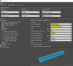
There is no special formula, you just need to estimate the line length and line width, and see if this gives a useful layout. Thicker substrate gives wider lines and more radiation loss, so this is a trade off. To show what you can expect, I created a quick filter design on 0.25mm FR4 and simulated this with 3D EM and realistic material properties. Thicker substrate resulted in layouts where lines are too wide relative to their length, which makes design even more difficult. Also check gap width - my design below requires 66µ gap, which is too small for normal PCB manufacturing.

fr4filter_design.PNG
fr4filter_2D.PNG
fr4filter_3D.PNG
fr4filter_results.PNG
 
Last edited:
Besides the FR4 problem, would it be advantageous to use a different topology than coupled line to make the design less critical to PCB structure width?
 

Besides the FR4 problem, would it be advantageous to use a different topology than coupled line to make the design less critical to PCB structure width?

I'm not a filter expert, and only had a quick look: Other shapes like hairpin looked bad, because the "folded" resonator length is rather small for these wide lines (at 0.25mm FR4). And interdigital resonators might be sensitive to manufacturing with the vias to ground. But as said, I'm only the simulation guy, not a filter designer.
 
Status
Not open for further replies.

Similar threads

Part and Inventory Search

Welcome to EDABoard.com

Sponsor

Back
Top