Continue to Site

Welcome to EDAboard.com

Welcome to our site! EDAboard.com is an international Electronics Discussion Forum focused on EDA software, circuits, schematics, books, theory, papers, asic, pld, 8051, DSP, Network, RF, Analog Design, PCB, Service Manuals... and a whole lot more! To participate you need to register. Registration is free. Click here to register now.

Layout Technique for Differential difference Amplifier

Status
Not open for further replies.

deveshkm

Member level 4
Joined
Jul 18, 2017
Messages
71
Helped
0
Reputation
0
Reaction score
0
Trophy points
6
Activity points
615
This is the schematic. i am doing the layout for this
Each transistor has 4 fingers each
The three transistors on the right are for dummy

pp pn np nn are gate inputs

A: pp B: pn
C: np D: nn

dda_schema.png

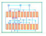
I am using the following scheme

ABBA (DUMMY) CDDC
DCCD (DUMMY) BAAB

The routing is quite complex.

The layout is not complete , yet
dda_layout.png

Please suggest better scheme or tips on layout for this.
 

Dummy M5 emplaces a capacitance between the pn-np & pp-nn branches. Is this intended? If so, why?
 

Dummy M5 emplaces a capacitance between the pn-np & pp-nn branches. Is this intended? If so, why?

I used this dummy to have one transistor which decouples left (M2 M3) and right side (M0 M1) transistors.
 

I used this dummy to have one transistor which decouples left (M2 M3) and right side (M0 M1) transistors.

I think M5's capacitance won't decouple, but couple the DDA nodes, so reduce the DDA's gain & intended functionality.

The dummies M4 & M28 - due to their capacitance - charge these nodes, and so reduce the gain - at least at high frequencies. Is this intended?
 

I think M5's capacitance won't decouple, but couple the DDA nodes, so reduce the DDA's gain & intended functionality.

The dummies M4 & M28 - due to their capacitance - charge these nodes, and so reduce the gain - at least at high frequencies. Is this intended?
No. Please suggest better scheme/references. I will add dummies, if required.
 

Your layout symmetry is fine, but dummies are needed only at the array ends, to keep the same environment also for the outside fingers:
(DUMMY)ABBACDDC(DUMMY)
(DUMMY)DCCDBAAB(DUMMY)​

The lengths of the dummy transistors may be shorter than those of the array fingers - important is only to keep the environment adjacent to the outside ends of the array.

Of course the routing will be complex. But try and keep max. symmetry for the routing, too, re. wire length ~ capacitance.

Connect all terminals of the 4 n-dummies to GND.

Perhaps you'll need bulk connections closer to the array transistors than your bulk ring. The DRC will tell you.

Don't connect the sources to the bulk ring - instead connect them directly to their respective nodes vss1, vss2, gnd (which might be the same node). Same for the bulk ring: no current should flow over the ring.
 

layout_CC_dda_amp.png

Please comment on this.
I am working other parts of the layout and will simulate after completing them
 

Please comment on this.

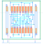
Following a sketchy glimpse your array looks good, even if I think you've wasted some space below and above it.

However your dummies aren't correctly positioned: dummies serve to guarantee a continuous environment, in this case for the 4 outside fingers of your array. That's why the spacing to the outside fingers and the position of the (gate) contacts should be the same as inside the array. This means the dummies should be incorporated into the array. As they are now, they don't serve their dummy purpose well - mainly because they are too far away.

Their shorter lengths (L) are fine, as I told you above. Important is the same spacing between the poly (gate) regions.
 

Status
Not open for further replies.

Part and Inventory Search

Welcome to EDABoard.com

Sponsor

Back
Top