E-design
Advanced Member level 5
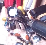
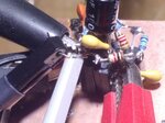
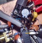
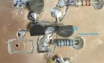
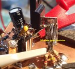
You could tighten-up your layout quite a lot. You don't want to have large diameter current loops if you want clean fast waveforms. You also want to minimize wiring inductances where possible.
- - - Updated - - -
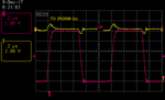
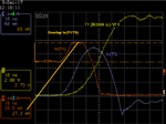
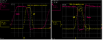
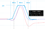
Some more waveforms.
- - - Updated - - -
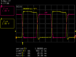
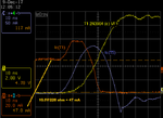
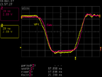
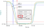
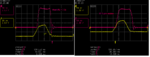
Some more waveforms.