Continue to Site

Welcome to EDAboard.com

Welcome to our site! EDAboard.com is an international Electronics Discussion Forum focused on EDA software, circuits, schematics, books, theory, papers, asic, pld, 8051, DSP, Network, RF, Analog Design, PCB, Service Manuals... and a whole lot more! To participate you need to register. Registration is free. Click here to register now.

Transceiver and SDI Interface

Status
Not open for further replies.

beginner_EDA

Full Member level 4
Joined
Aug 14, 2013
Messages
191
Helped
0
Reputation
0
Reaction score
0
Trophy points
1,296
Activity points
3,854
To route data from one SDI Channel to another

Hi,
How to route SDI data coming on one channel as RX via MGT transceiver pin to another SDI Channel as TX also via MGT transceiver pin.

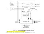
I am using following reference design:
https://www.xilinx.com/support/docu...s/xapp592-smpte-sdi-w-k7-gtx-transceivers.pdf
here data in (RX) and data out (TX) are on same channel (channel 0). I am using SDI Pass-Through mode.

But I would like to route data coming from one channel to another channel i.e. RX at channel 0 and TX at channel 1.

only providing corresponding MGT Transceiver pin didn't work. i.e. RX transceiver pin for channel 0 and TX trabsceiver pin for channel 1.

Any Idea?
 

Re: To route data from one SDI Channel to another

Referring only to Figure 1 @ Pg2:

Route the complete bunch of Tx chnl0 to Rx chnl1 and Rx chnl0 to Tx chnl1. Be careful about the separate Tx and Rx clocks.
 

Re: To route data from one SDI Channel to another

You might have better luck not splitting the design as you are attempting. Use the design as-is. Instantiate two of them using the appropriate transceiver location constraints, use only the transmit on one of the instances (stubbing off any unused RX user interface inputs) and use only the receiver on the other instance (stubbing of all the TX user interface inputs).
 

Re: To route data from one SDI Channel to another

This design uses the pi xco feature of the cpll. So both reference clocks need to make it to the target gtx quad. There are rules for how far a clock can be routed inside the fpga. You may need to create dummy tiles if routing more than one quad.

So step 1 is determining which quads the TX and rx transceivers are in. Then fining how to get the refund clocks there.
 

Re: To route data from one SDI Channel to another

Instantiate two of them using the appropriate transceiver location constraints, use only the transmit on one of the instances (stubbing off any unused RX user interface inputs) and use only the receiver on the other instance (stubbing of all the TX user interface inputs).
Hi,
I instatntiated 2 SDI Channel as you mentioned:

Code Verilog - [expand]
1
2
3
4
5
6
7
8
9
10
11
12
13
14
15
16
17
18
19
20
21
22
23
24
25
26
27
28
29
30
31
32
33
34
35
36
37
38
39
40
41
42
43
44
45
46
47
48
49
50
51
52
53
54
55
56
57
58
59
60
61
62
63
64
65
66
67
68
69
70
71
72
73
74
75
76
77
78
79
80
81
82
83
84
85
86
87
88
89
90
91
92
93
94
95
96
97
98
99
100
101
102
103
104
105
106
107
108
109
110
111
112
113
114
115
116
117
118
119
120
121
122
123
124
125
126
127
128
129
130
131
132
133
134
135
136
137
138
139
140
141
142
143
144
145
146
147
148
149
150
151
152
153
154
155
156
157
158
159
160
161
162
163
164
165
166
167
168
169
170
171
172
173
174
175
176
177
smpte_sdi SDIRX (     // Edit this line to instance the name of the core as generated by CORE Generator
    .rx_rst             (rx_rst | ~rx_change_done_s),
    .rx_usrclk          (rx_usrclk),
    .rx_data_in         (rx_rxdata),
    .rx_sd_data_in      (rx_sd_rxdata),
    .rx_sd_data_strobe  (rx_sd_data_strobe),
    .rx_frame_en        (rx_frame_en),
    .rx_mode_en         (rx_mode_en),
    .rx_mode            (rx_mode_int),
    .rx_mode_hd         (rx_mode_hd),
    .rx_mode_sd         (rx_mode_sd),
    .rx_mode_3g         (rx_mode_3g),
    .rx_mode_detect_en  (1'b1),
    .rx_mode_locked     (rx_mode_locked),
    .rx_forced_mode     (2'b00),
    .rx_bit_rate        (rx_m),
    .rx_t_locked        (rx_t_locked),
    .rx_t_family        (rx_t_family),
    .rx_t_rate          (rx_t_rate),
    .rx_t_scan          (rx_t_scan),
    .rx_level_b_3g      (rx_level_b_3g),
    .rx_ce_sd           (rx_ce_sd),
    .rx_nsp             (rx_nsp),
    .rx_line_a          (rx_line_a),
    .rx_a_vpid          (rx_a_vpid),
    .rx_a_vpid_valid    (rx_a_vpid_valid),
    .rx_b_vpid          (rx_b_vpid),
    .rx_b_vpid_valid    (rx_b_vpid_valid),
    .rx_crc_err_a       (rx_crc_err_a),
    .rx_ds1a            (rx_ds1a),
    .rx_ds2a            (rx_ds2a),
    .rx_eav             (rx_eav),
    .rx_sav             (rx_sav),
    .rx_trs             (rx_trs),
    .rx_line_b          (rx_line_b),
    .rx_dout_rdy_3g     (rx_dout_rdy_3g),
    .rx_crc_err_b       (rx_crc_err_b),
    .rx_ds1b            (rx_ds1b),
    .rx_ds2b            (rx_ds2b),
    .rx_edh_errcnt_en   (rx_edh_errcnt_en),
    .rx_edh_clr_errcnt  (rx_edh_clr_errcnt),
    .rx_edh_ap          (rx_edh_ap),
    .rx_edh_ff          (rx_edh_ff),
    .rx_edh_anc         (rx_edh_anc),
    .rx_edh_ap_flags    (rx_edh_ap_flags),
    .rx_edh_ff_flags    (rx_edh_ff_flags),
    .rx_edh_anc_flags   (rx_edh_anc_flags),
    .rx_edh_packet_flags(rx_edh_packet_flags),
    .rx_edh_errcnt      (rx_edh_errcnt),
 
    .tx_rst             (),
    .tx_usrclk          (),
    .tx_ce              (),
    .tx_din_rdy         (),
    .tx_mode            (),
    .tx_level_b_3g      (),
    .tx_insert_crc      (),
    .tx_insert_ln       (),
    .tx_insert_edh      (),
    .tx_insert_vpid     (),
    .tx_overwrite_vpid  (),
    .tx_video_a_y_in    (),
    .tx_video_a_c_in    (),
    .tx_video_b_y_in    (),
    .tx_video_b_c_in    (),
    .tx_line_a          (),
    .tx_line_b          (),
    .tx_vpid_byte1      (),
    .tx_vpid_byte2      (),
    .tx_vpid_byte3      (),
    .tx_vpid_byte4a     (),
    .tx_vpid_byte4b     (),
    .tx_vpid_line_f1    (),
    .tx_vpid_line_f2    (),
    .tx_vpid_line_f2_en (),
    .tx_ds1a_out        (),
    .tx_ds2a_out        (),
    .tx_ds1b_out        (),
    .tx_ds2b_out        (),
    .tx_use_dsin        (),
    .tx_ds1a_in         (),
    .tx_ds2a_in         (),
    .tx_ds1b_in         (),
    .tx_ds2b_in         (),
    .tx_sd_bitrep_bypass(),
    .tx_txdata          (),
    .tx_ce_align_err    ());


    smpte_sdi SDITX (     // Edit this line to instance the name of the core as generated by CORE Generator
        .rx_rst             (),
        .rx_usrclk          (),
        .rx_data_in         (),
        .rx_sd_data_in      (),
        .rx_sd_data_strobe  (),
        .rx_frame_en        (),
        .rx_mode_en         (),
        .rx_mode            (),
        .rx_mode_hd         (),
        .rx_mode_sd         (),
        .rx_mode_3g         (),
        .rx_mode_detect_en  (),
        .rx_mode_locked     (),
        .rx_forced_mode     (),
        .rx_bit_rate        (),
        .rx_t_locked        (),
        .rx_t_family        (),
        .rx_t_rate          (),
        .rx_t_scan          (),
        .rx_level_b_3g      (),
        .rx_ce_sd           (),
        .rx_nsp             (),
        .rx_line_a          (),
        .rx_a_vpid          (),
        .rx_a_vpid_valid    (),
        .rx_b_vpid          (),
        .rx_b_vpid_valid    (),
        .rx_crc_err_a       (),
        .rx_ds1a            (),
        .rx_ds2a            (),
        .rx_eav             (),
        .rx_sav             (),
        .rx_trs             (),
        .rx_line_b          (),
        .rx_dout_rdy_3g     (),
        .rx_crc_err_b       (),
        .rx_ds1b            (),
        .rx_ds2b            (),
        .rx_edh_errcnt_en   (),
        .rx_edh_clr_errcnt  (),
        .rx_edh_ap          (),
        .rx_edh_ff          (),
        .rx_edh_anc         (),
        .rx_edh_ap_flags    (),
        .rx_edh_ff_flags    (),
        .rx_edh_anc_flags   (),
        .rx_edh_packet_flags(),
        .rx_edh_errcnt      (),
    
        .tx_rst             (tx_rst),
        .tx_usrclk          (tx_usrclk),
        .tx_ce              (tx_ce),
        .tx_din_rdy         (tx_din_rdy),
        .tx_mode            (tx_mode),
        .tx_level_b_3g      (tx_level_b_3g),
        .tx_insert_crc      (tx_insert_crc),
        .tx_insert_ln       (tx_insert_ln),
        .tx_insert_edh      (tx_insert_edh),
        .tx_insert_vpid     (tx_insert_vpid),
        .tx_overwrite_vpid  (tx_overwrite_vpid),
        .tx_video_a_y_in    (tx_video_a_y_in),
        .tx_video_a_c_in    (tx_video_a_c_in),
        .tx_video_b_y_in    (tx_video_b_y_in),
        .tx_video_b_c_in    (tx_video_b_c_in),
        .tx_line_a          (tx_line_a),
        .tx_line_b          (tx_line_b),
        .tx_vpid_byte1      (tx_vpid_byte1),
        .tx_vpid_byte2      (tx_vpid_byte2),
        .tx_vpid_byte3      (tx_vpid_byte3),
        .tx_vpid_byte4a     (tx_vpid_byte4a),
        .tx_vpid_byte4b     (tx_vpid_byte4b),
        .tx_vpid_line_f1    (tx_vpid_line_f1),
        .tx_vpid_line_f2    (tx_vpid_line_f2),
        .tx_vpid_line_f2_en (tx_vpid_line_f2_en),
        .tx_ds1a_out        (tx_ds1a_out),
        .tx_ds2a_out        (tx_ds2a_out),
        .tx_ds1b_out        (tx_ds1b_out),
        .tx_ds2b_out        (tx_ds2b_out),
        .tx_use_dsin        (tx_use_dsin),
        .tx_ds1a_in         (tx_ds1a_in),
        .tx_ds2a_in         (tx_ds2a_in),
        .tx_ds1b_in         (tx_ds1b_in),
        .tx_ds2b_in         (tx_ds2b_in),
        .tx_sd_bitrep_bypass(1'b0),
        .tx_txdata          (tx_txdata),
        .tx_ce_align_err    (tx_ce_align_err));


but didn't understand the transceiver pins connection. Because transceiver pins are connected to another independent entity:

Code Verilog - [expand]
1
2
3
4
5
6
7
8
9
10
11
12
13
14
15
16
17
18
19
20
21
22
23
24
25
26
27
28
29
30
31
32
33
34
35
36
37
38
39
40
41
42
43
44
45
46
47
48
49
50
51
52
53
54
55
56
57
58
59
60
61
62
63
64
65
66
67
68
69
70
71
72
73
74
75
//------------------------------------------------------------------------------
// GTX transceiver
//
k7gtx_sdi_wrapper_GT #(
    .GT_SIM_GTRESET_SPEEDUP         ("FALSE"))
GTX_i (
    .cpllfbclklost_out              (),
    .cplllock_out                   (cplllock_int),
    .cplllockdetclk_in              (clk),
    .cpllrefclklost_out             (),
    .cpllreset_in                   (cpllreset),
 
    .gtgrefclk_in                   (cpll_grefclk),
    .gtnorthrefclk0_in              (cpll_north0),
    .gtnorthrefclk1_in              (cpll_north1),
    .gtrefclk0_in                   (cpll_refclk0),
    .gtrefclk1_in                   (cpll_refclk1),
    .gtsouthrefclk0_in              (cpll_south0),
    .gtsouthrefclk1_in              (cpll_south1),
 
    .drpaddr_in                     (drpaddr),
    .drpclk_in                      (drpclk),
    .drpdi_in                       (drpdi),
    .drpdo_out                      (),
    .drpen_in                       (drpen),
    .drprdy_out                     (drprdy),
    .drpwe_in                       (drpwe),
    .qpllclk_in                     (qpllclk),
    .qpllrefclk_in                  (qpllrefclk),
    .txsysclksel_in                 (tx_sysclksel),
    .dmonitorout_out                (),
    .loopback_in                    (3'b000),
    .rxrate_in                      (rx_rate),
    .eyescanreset_in                (1'b0),
    .rxuserrdy_in                   (rx_userrdy),
    .eyescandataerror_out           (),
    .eyescantrigger_in              (1'b0),
    .rxcdrhold_in                   (rx_cdrhold),
    .rxusrclk_in                    (rx_usrclk),
    .rxusrclk2_in                   (rx_usrclk),
    .rxdata_out                     (rx_rxdata),
   [B] .gtxrxp_in                      (rxp),
    .gtxrxn_in                      (rxn),[/B]
    .rxbufreset_in                  (1'b0),
    .rxbufstatus_out                (),
    .rxlpmhfhold_in                 (1'b0),
    .rxlpmlfhold_in                 (1'b0),
    .rxdfelpmreset_in               (1'b0),
    .rxmonitorout_out               (),
    .rxmonitorsel_in                (2'b00),
    .rxratedone_out                 (),
    .rxoutclk_out                   (rx_outclk),
    .gtrxreset_in                   (rx_gtrxreset),
    .rxpmareset_in                  (1'b0),
    .rxresetdone_out                (rx_resetdone),
    .txpostcursor_in                (5'b00000),
    .txprecursor_in                 (5'b00000),
    .gttxreset_in                   (tx_gttxreset),
    .txuserrdy_in                   (tx_userrdy),
    .txusrclk_in                    (tx_usrclk),
    .txusrclk2_in                   (tx_usrclk),
    .txrate_in                      (tx_rate),
    .txbufstatus_out                (tx_bufstatus),
    .txdiffctrl_in                  (4'b1000),
    .txdata_in                      (tx_txdata),
[B]    .gtxtxn_out                     (txn),
    .gtxtxp_out                     (txp),[/B]
    .txoutclk_out                   (tx_outclk),
    .txoutclkfabric_out             (),
    .txoutclkpcs_out                (),
    .txratedone_out                 (tx_ratedone),
    .txpcsreset_in                  (tx_bufstatus[1]),
    .txpmareset_in                  (1'b0),
    .txresetdone_out                (tx_resetdone)
);


but when I try to assign transceiver pins (see bold part) for RX from one channel and TX from another channel, it shows strange things. Although I can write it in XDC file but When I look on I/O pin planning it is automatically assigned pins from same channel. i.e. When I take RX pin from channel 0, it automatically take TX pin from channel 0. i.e. I can not assign manually here. May be because it is dedicated I don't know. Where should I assigned then TX pin from different channel.

I am also getting following critical warning:
[Place 30-143] Sub-optimal placement for an IBUFDS / GT component pair. Processing will continue as all instances of this rule have been LOCed.
TXMGTCLKIN (IBUFDS_GTE2.O) is locked to IBUFDS_GTE2_X0Y2
and SDI0/SDI/GTX_i/gtxe2_i (GTXE2_CHANNEL.GTREFCLK1) is locked to GTXE2_CHANNEL_X0Y12
 

Re: To route data from one SDI Channel to another

That is not what I suggested...you still seem to be breaking the logic up for a generated core. Though you might have to generate only one core with two channels (this is the case now with most of the newer parts as they have quads that contain a common PLL block).

I suggested if you are using a GTXE2_CHANNEL (0) RX and GTXE2_CHANNEL (1) TX then you would create two separate cores, then you would connect only the RX user side for the first core and the TX user side for the second core. This is based on the first post where it appears you want to only use the RX side of a MGT for channel 0 and the TX side of an MGT for channel 1 (note: the TX of channel 0 is unused and the RX of channel 1 is unused).

It is also likely we don't understand what you are trying to do (not how you are trying to do this). The how is obviously broken, so what are you attempting to do? What is the structure of the design how is it supposed to interconnect with other things? A drawing could have help originally, I suspect you are attempting something that cannot be done give the restrictions of the FPGA, or you don't understand what you can do and how it applies to implementation on the FPGA.
 

Re: To route data from one SDI Channel to another

The warning is pretty clear.

You would need to look at the datasheet or such in order to see where the tiles are. In the 7-series, you have two clock inputs per quad-tile. These can also route to a quad above and a quad below. IIRC, this is in the gtx common. I think you can route two clocks up/down.

In this application, there is a lot of logic for selecting the clocks for the qpll (for rx) and the cpll (for tx). The design uses the "phase-interpolation controlled oscillator" feature of the cpll. This allows you to match the tx clock to the recovered rx clock.

You might also need to look at any form of dynamic-reconfiguration port fsm, as the rx and tx are now in different locations. likewise, there may need to be some changes to the reset logic.
 

Hi,
In attachment there is block diagram(page 9) of Xilinx SDI core accompanied by Transceiver.
https://www.xilinx.com/support/documentation/ip_documentation/v_smpte_sdi/v1_0/pg071-v-smpte-sdi.pdf

For just SDI In and SDI Out as in pass through mode:
https://www.xilinx.com/support/docu...s/xapp592-smpte-sdi-w-k7-gtx-transceivers.pdf


I believe transceiver common block and channel is configured as mentioned in page 41:
https://www.xilinx.com/support/documentation/user_guides/ug476_7Series_Transceivers.pdf

but I didn't understand how Transceiver common and channel block is working here? Any Explanation?

If I increase SDI channel from 1 to 2 by instantiating 2 SDI IP core, do I also need to configure another Transceiver common and channel block? or I can use the same transceiver. If so how I can configure them? Honestly I didn't understand how transceiver is working with SDI channel. Any explanation?
 

Attachments

  • sdigtx.jpg
    sdigtx.jpg
    121.9 KB · Views: 68

I'll answer based on your past posts. SDI is a "Plesiochronous " system (wanting to be a synchronous system). It means the rate is "near" some defined rate, but not exact. However, the standard also expects one transmitter to transmit to one receiver with no idle data. If you want to be a middle-man, you have to match the actual tx rate to the actual rx rate.

On the RX side, there is a "Clock-Data-Recovery" circuit (CDR) that generates the RxRecClk. The recovered clock is close to the reference clock.

On the TX side, there is the "Phase-Interpolated Controlled Oscillator" (PI-XCO) to generate the exact same rate in a way compatible with the requirements of the FPGA.

The QPLL doesn't have the PI-XCO features, but the CPLL does. So, for RX everything is based on the QPLL. For Tx, everything is based on CPLL.

The rest of the pdf is based on the different rates of SDI.
 

Status
Not open for further replies.

Part and Inventory Search

Welcome to EDABoard.com

Sponsor

Back
Top