Continue to Site

Welcome to EDAboard.com

Welcome to our site! EDAboard.com is an international Electronics Discussion Forum focused on EDA software, circuits, schematics, books, theory, papers, asic, pld, 8051, DSP, Network, RF, Analog Design, PCB, Service Manuals... and a whole lot more! To participate you need to register. Registration is free. Click here to register now.

LNA biasing with current mirror

Status
Not open for further replies.

saipakala

Newbie level 4
Joined
Nov 30, 2016
Messages
6
Helped
0
Reputation
0
Reaction score
0
Trophy points
1
Activity points
33
respected sir/madam

i am designing a LNA in that i am having doubt i had following lines in my reference paper

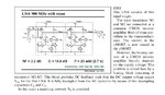
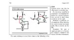
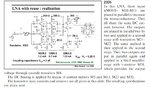
"""The LNA is biased by means of a current mirror"""

""transistor is biased through one ac-ground point of the filter"".

can you please help anyone
 

Hi,

I know nothing about LNAs, so apologies if the answer is wrong/unrelated to the two questions, or just plain unhelpful, these three pages are from Analog Design Essentials, I hope they are of some use.
 

Attachments

  • lna 1.JPG
    lna 1.JPG
    97.2 KB · Views: 150
  • lna 2.JPG
    lna 2.JPG
    73.2 KB · Views: 129
  • lna 3.JPG
    lna 3.JPG
    118.5 KB · Views: 133

Thanks for your concern sir.
but those are not helpful for me.
actually what they are saying means LNA is biasied by current mirror. so i am not able to do that.
if you have any idea please help me
 

Hi,

As I said, I know nothing about LNAs. Trying to help, I can only guess that "The LNA is biased by means of a current mirror" could mean that, looking at slide "lna 3," maybe R1, and possibly, R2 and R3 also could be replaced with a current mirror/current mirrors of your choice, i.e. replacing a passive load with an active load, if that's what those resistors are doing. And maybe I have misinterpreted the function of those resistors, maybe they are filters. Couldn't comment on the lower half of the schematic.

If you have a basic design sketched out, can you see places where you can replace passive loads with active loads? Perhaps not the same, but thinking of op amps, they are biased with current mirrors rather than resistors to set the bias currents.

"transistor is biased through one ac-ground point of the filter" - hopefully another member who designs LNAs will be able to help you if they are familiar with this idea, but without a schematic it might be hard for other members to guess what you are asking about - which filter, where is it in your design? e.g. I'll ask you: Where do I put the compensation around an SMPS op amp in my design, saipakala? - Without seeing the circuit it's not easy, is it? :)

Good luck!
 

sir first of all thanks for your detailed explanation.
i have uploaded the circiut design..
in that u can see that "Vbias" at the bottom of filter component. so if you have any idea tell me sir i am waiting for your explanation

Untitled.png
 

Hi saipakala,

Thanks for uploading schematic. It depends on the bias voltage required, and also if you are using discrete components or are designing an IC. I think you could try using a bandgap, or an adjustable bandgap for >1.2V, or any reference of the right voltage if it's a discrete circuit, but they will all have a little drift over temp, maybe 20mV across range. If you are designing your own, from what I've seen of op amps, some of the bias voltages are taken from current mirrors (as you said in post #1: "The LNA is biased by means of a current mirror"). Poor quality bias voltages could be stacked diodes or a resistor divider, which I don't recommend.

See if the pdf document in post #3 in this thread helps: bias voltage independent with temperature, if not we can think of something else.

What's the supply voltage? Maybe a Full Wilson current mirror would be a good choice.
 
apologize for late reply

Sir i have tried with some band gap reference circuits what you have suggested me in the above thread, it is okay some what useful thanks for that sir.And with in a short period i will try to upload my schematic.

While coming to supply voltage if I am using 180nm technolgy in my IC design generally it will be 1.8V. so i am using that. I don't know either it will be wrong or right.
 

Status
Not open for further replies.

Part and Inventory Search

Welcome to EDABoard.com

Sponsor

Back
Top