Continue to Site

Welcome to EDAboard.com

Welcome to our site! EDAboard.com is an international Electronics Discussion Forum focused on EDA software, circuits, schematics, books, theory, papers, asic, pld, 8051, DSP, Network, RF, Analog Design, PCB, Service Manuals... and a whole lot more! To participate you need to register. Registration is free. Click here to register now.

Picoblaze Spartan 3E I2C

Status
Not open for further replies.

FecP

Newbie level 6
Joined
Oct 17, 2016
Messages
14
Helped
0
Reputation
0
Reaction score
0
Trophy points
1
Activity points
160
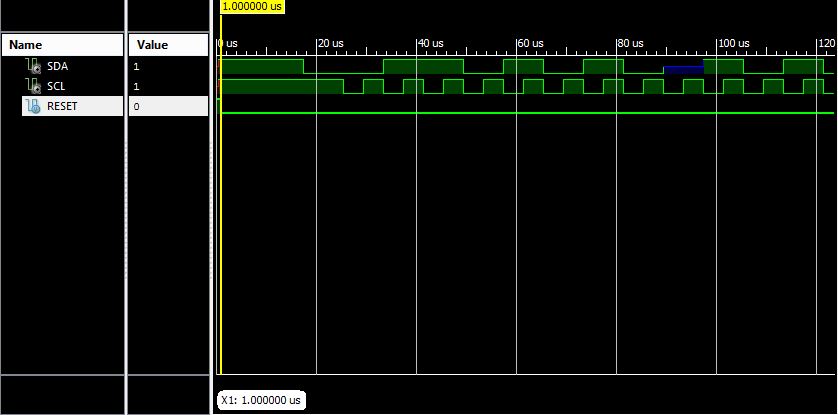
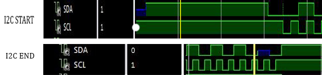
I have to implement 400 KHz I2C on a Spartan 3E , and am considering using the PICOBLAZE controller for the purpose.However, I wanted to ask if there's anything equivalent to the tri state buffer in the PICOBLAZE instruction set.I need something to allow the reception of the acknowledge signal from the slave, which would normally require an I/O (Bi-directional) pin.
 

If you are using Picoblaze then you are going to have to bit-bang the I2C interface, just include as part of your GPIO a tristate enable, output data, input data, and clock.

In Verilog something like this:

Code Verilog - [expand]
1
2
3
4
5
6
7
8
9
10
inout  sda,
output scl
 
wire [3:0] pico_gpio
 
// These two lines will synthesize to a tristate buffer.
assign sda = pico_gpio[2] ? 1'bz : pico_gpio[0];  // gpio[2] is the tristate control.
assign pico_gpio[1] = sda;
 
assign scl = pico_gpio[3];


pico_gpio is the register you create to bit bang the I2C. Three bits are outputs from the Picoblaze and one is an input the Picoblaze.
 
  • Like
Reactions: FecP

    FecP

    Points: 2
    Helpful Answer Positive Rating
Thank you for the prompt reply! I understand that the Picoblaze essentially uses 4 bits at a time.One for clock, one for SDA, one for tristate control and one for inputting ack signals.So, when I am expecting an ack from the slave, I'll have to set
Code:
pico_gpio[2]
to allow the SDA line to be pulled low.I can't help but think that using a faster clock than the minimum 800KHz on the Picoblaze would ease the timing constraints.
 

A Picoblaze should be able to run way faster than 800 KHz, it should work fine at 10's of MHz.

You would be better off using a DCM and a clock frequency that is the minimum for the DCM and then use clock enables to "divide" down that clock to get your 400KHz I2C frequency. This will be an 18-280 MHz input clock with a divide down on the CLKDV output that is used to run the counter for your clock enable.

This way if this I2C needs to interface with the rest of your FPGA it can do so without resorting to asynchronous interfaces as the clocks for both the reset of the logic and the I2C are all coming from a single DCM, just make sure the DCM isn't producing some non-integer multiple between the two clocks (CLKDIV and CLK0). The timing between the two clocks will be constrained according to the faster of the two clocks and you won't require adding extra synchronization logic to communicate between the two domains.
 
  • Like
Reactions: FecP

    FecP

    Points: 2
    Helpful Answer Positive Rating
I2C Master Code Verification Spartan 3-E

I have to implement I2C to configure a component on start up ; hence, the FPGA board need only be operated in the Master Mode.I ave written code which divides the incoming clock to produce a frequency of around 390,000 Khz (391.625) .The component (ADV7171) datasheet recommends an I2C frequency lower than 400 Khz.


I have simulated the code in ISIM and it appears to be working ; however, the testing here is limited because I can't receive an ACK bit. Anyway, is there any way to test this code?

DOUBTS:
1.I will constrain the SDA and SCL pins to be normal pull up pins.Will this remove the necessity of declaring an inout SDA pin?
2.I make the 9th bit on the SDA 1'bz to receive an ACK signal.Will this work?
3.Is there some way I could simulate the entire process before implementing it?


CODE :

Code:
module I2Cagain(    input CLK,
					 input RESET,
					 output SDA,            //Pullup SDA and SCL in UCF
					 output SCL
					);

reg SCLreg;
reg SDA_R;
reg [2 : 0] counter;                  //Divide Incoming Clock
reg [4 : 0] I2C_COUNTER;              //All I2C write cases
	always @ (posedge CLK)
begin
	if(RESET)
	begin 
	counter <= 0; 
	SCLreg <= 0; 
	I2C_COUNTER <=0; 
	SDA_R <= 1;
	end
	else
	begin
	counter <= counter + 1;
	SCLreg <= counter[2];
	if(counter == 7)
	I2C_COUNTER	 <= I2C_COUNTER + 1;
	case (I2C_COUNTER)
	1  : SDA_R <= 1'b1;  //START
	2  : SDA_R <= 0;    	//Low Transition, START
	3  : SDA_R <= 0;
	4  : SDA_R <= 1;
	5  : SDA_R <= 1;
	6  : SDA_R <= 0;
	7  : SDA_R <= 1;
	8  : SDA_R <= 0;
	9  : SDA_R <= 1;
	10 : SDA_R <= 0;
	11 : SDA_R <= 1'bz;
	12 : SDA_R <= 1'b1;
	13 : SDA_R <= 0;    	
	14 : SDA_R <= 1;
	15 : SDA_R <= 0;
	16 : SDA_R <= 1;
	17 : SDA_R <= 0;
	18 : SDA_R <= 1;
	19 : SDA_R <= 0;
	20 : SDA_R <= 1'bz;
	21 : SDA_R <= 0;
	22 : SDA_R <= 1;
	23 : SDA_R <= 1;
	24 : SDA_R <= 0;
	25 : SDA_R <= 1;
	26 : SDA_R <= 0;
	27 : SDA_R <= 1;
	28 : SDA_R <= 1;
	29 : SDA_R <= 1'bz;
	30 : SDA_R <= 0;             ///STOP
	31 : SDA_R <= 1;             ///0 to 1 or 1'bz, STOP 
	endcase
	end
end
	assign SCL = (I2C_COUNTER)> 2 && (I2C_COUNTER)< 31 ? SCLreg : 1'b1; //Internal pull up, clock need not be driven to 1?.
	assign SDA = SDA_R;
endmodule


Re: I2C Master Code Verification Spartan 3-E

I have simulated the code in ISIM and it appears to be working ; however, the testing here is limited because I can't receive an ACK bit. Anyway, is there any way to test this code?
Yes it's called a testbench, learn to write one.

DOUBTS:
1.I will constrain the SDA and SCL pins to be normal pull up pins.Will this remove the necessity of declaring an inout SDA pin?
no, if SDA is an output only you won't be able to read the ACK returned by the slave as the output will always be driving the pin high or low.

2.I make the 9th bit on the SDA 1'bz to receive an ACK signal.Will this work?
No, you really don't understand you are designing hardware, draw a schematic of the design. Until you know how to draw a schematic you won't know how to design Verilog hardware.

3.Is there some way I could simulate the entire process before implementing it?
Yeah it's called a testbench, which is just another file that you instantiate your DUT in and that file you can write Verilog programs to test your desgin.

I doubt your case statement will synthesize correctly. The Z's won't be generated as you've specified.

I already showed you the way to implement an SDA inout pin in post #2. Use it.

You should also use a shift register instead of a big mux to send the data out the SDA pin instead of the ridiculous case statement and counter. The counter should be there to tell you how long to shift not as a mux select. Verilog is a Hardware Description Language (HDL) it should not be written like a programming language.
 

Re: I2C Master Code Verification Spartan 3-E

Thank you for yet another detailed reply! I apologize for my crude behaviour. Rest assured, I will not repeat it. I am now using cascadable Shift Registers to implement I2C. As mentioned earlier, I want to sample the ACK bit and toggle an LED(or any visual expression) to make certain that the I2C is functioning as intended.
For this purpose, I sample the SDA pin on first posedge of SCL after the negedge at which SDA goes to high impedance via the tristate buffer. The approach has not worked.

I am attaching the part of the code where I check for ACK bit and the I2C start and stop conditions in an image.


Code:
	counter <= counter + 1;
	SCLreg  <= counter[4];       //MSB of SCLreg = SCL
	if(counter == 31)           
	Clk_Enable <= 1;
	else if(counter == 16)      
	Clk_Enable_Ack <= 1;
	else
	begin
	Clk_Enable <= 0;
	Clk_Enable_Ack <= 0;
	end
	assign ACK = Clk_Enable_Ack? (IO)? !SDA : 1'b0 : 1'b0;
//IF ACK does go high, an LED will toggle from 1 to zero and STAY at zero.
 

Status
Not open for further replies.

Part and Inventory Search

Welcome to EDABoard.com

Sponsor

Back
Top