papaisou11
Member level 2
I am working on a project where I need to measure the current drawn by multiple loads from a single power supply using a 8-bit PIC micro-controller. Also, when an overload condition is detected in any of the loads, I need to cut it off using a MOSFET. Here, each port is limited to a specific current and the sum of all the port current is the total rating of the power supply.
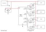
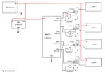
To do this I have setup the circuit as shown below.
Here I have 4 output ports of the power supply and 4 loads are connected to them. I am using a MOSFET and a 1-Ohm shunt resistor on each port to measure the current drawn.
Firstly, when I connect 1 load (LOAD1) the circuit works as expected. Here the load is variable dummy load. For this configuration I am getting good readings. I verified the reading with a multi-meter.
When I connect a second load the problem starts. I keep the 2nd load’s current at a constant level by using an LED as LOAD2. Now when I increase/decrease the 1st load, I find changes in reading of the 2nd load. The value increases with increase in current from the 1st load and vice versa when the current decreases.
Example:
- LOAD1 = 200mA, LOAD2 = 20mA
- LOAD1 = 350mA, LOAD2 = 40mA
- LOAD1 = 600mA, LOAD2 = 100mA
I find the same readings in the multi-meter also. I am measuring voltage across the 1 Ohm resistor with the multi-meter. But I found proper readings, i.e. 1st load current changes and 2nd load remains constant, when I connected the multi-meter as an ammeter, i.e. in series with the circuit.
I think the problem is in the way I am measuring the current. Can anyone provide some insights on how this should actually be done?
Any comment or help is highly appreciated.
Thanks for reading.


