Continue to Site

Welcome to EDAboard.com

Welcome to our site! EDAboard.com is an international Electronics Discussion Forum focused on EDA software, circuits, schematics, books, theory, papers, asic, pld, 8051, DSP, Network, RF, Analog Design, PCB, Service Manuals... and a whole lot more! To participate you need to register. Registration is free. Click here to register now.

ADS 2012 substrate for CPW line

Status
Not open for further replies.

alice12

Newbie level 4
Joined
Apr 28, 2016
Messages
7
Helped
0
Reputation
0
Reaction score
0
Trophy points
1
Activity points
65
Hello,

I am simulating on momentum/ADS 2012 a CPW transmission line with finite ground planes.

I am wondering if my substrate is well defined.
I selected :
- for the top layer: strip layer (I define then two ports connected to the conductor and I associate to them their 4 ground ports (2 for each one))
- for the conductor: sheet (operation)
- for the bottom layer: strip layer (I have better results than the case slot layer and I don't understand why and how can I choose)
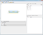
- It's Cu printed on FR4. So I have chosen H=1.6 mm and T=35 µm.

You can find the photo of my substrate attached.
Can you please confirm that I haven't any mistake?

Thank you !!

Alice. subtrate.PNG
 

Hello,

I am simulating on momentum/ADS 2012 a CPW transmission line with finite ground planes.

I am wondering if my substrate is well defined.
I selected :
- for the top layer: strip layer (I define then two ports connected to the conductor and I associate to them their 4 ground ports (2 for each one))
- for the conductor: sheet (operation)
- for the bottom layer: strip layer (I have better results than the case slot layer and I don't understand why and how can I choose)
- It's Cu printed on FR4. So I have chosen H=1.6 mm and T=35 µm.

You can find the photo of my substrate attached.
Can you please confirm that I haven't any mistake?

Thank you !!

Alice. View attachment 129710

1.6mm distance to reference plane is very large. What is your trace width? Trace weight/thickness is 35 um? Also, I do not see coplanar gap to coplanar reference plane for your CBCPW. See attached photo:

CBCPW.png
 

Hello,

I am simulating on momentum/ADS 2012 a CPW transmission line with finite ground planes.

I am wondering if my substrate is well defined.
I selected :
- for the top layer: strip layer (I define then two ports connected to the conductor and I associate to them their 4 ground ports (2 for each one))
- for the conductor: sheet (operation)
- for the bottom layer: strip layer (I have better results than the case slot layer and I don't understand why and how can I choose)
- It's Cu printed on FR4. So I have chosen H=1.6 mm and T=35 µm.

You can find the photo of my substrate attached.
Can you please confirm that I haven't any mistake?

Thank you !!

Alice. View attachment 129710
You have to close your substrate with a proper GND plane at bottom.
 

Are you using ADS 2012 ? because we haven't the same interface.
In my case I can't change the conductor.

For 1.6mm, it is the thickness of my substrate (FR4) and 35 µm the conductor's thickness (copper).
 

Are you using ADS 2012 ? because we haven't the same interface.
In my case I can't change the conductor.

For 1.6mm, it is the thickness of my substrate (FR4) and 35 µm the conductor's thickness (copper).

70 mils is typical for a MLB thickness (total thickness of the board), not for the distance to reference plane from a transmission line. In your case, a CPW. There will be no fringe-field coupling to your reference plane if it is 1.6mm away. You need to have your transmission line (CPW) with some dielectric gap to the coplanar reference plane (GND). In your TLINE editor picture above, it looks as though you have a single piece of metal floating. With no adjacent and or coplanar reference/return paths. This is effectively not a transmission line. This is most likely why you have a strange impedance value. Your stack-up dimensions also look very strange/wrong. Albeit, I do not know what you're trying to accomplish.

What is the desired trace width and impedance you're trying to achieve? Is it a CPW, or CBCPW you're attempting to model? If possible, what is the application frequency of interest?

I'm using ADS 2016. But 2012 has the capability to create CPW and or CBCPW.
 

70 mils is typical for a MLB thickness (total thickness of the board), not for the distance to reference plane from a transmission line. In your case, a CPW. There will be no fringe-field coupling to your reference plane if it is 1.6mm away.

I don't understand why 70mils (=1,778 mm). I have a totale thickness = 1,6 + 0,035 mm.

You need to have your transmission line (CPW) with some dielectric gap to the coplanar reference plane (GND). In your TLINE editor picture above, it looks as though you have a single piece of metal floating. With no adjacent and or coplanar reference/return paths. This is effectively not a transmission line. This is most likely why you have a strange impedance value. Your stack-up dimensions also look very strange/wrong.

But, with ADS 2012, in substrate definition, how can I change the conductor to 2 pieces ? It's always one piece on the substrate definition, and, in the layout I use three conductors, two of them are ground planes.
In a CPW line, the only GND plane is on the same (top) layer. I haven't another reference plane since there isn't a bottom layer.


Albeit, I do not know what you're trying to accomplish.
What is the desired trace width and impedance you're trying to achieve? Is it a CPW, or CBCPW you're attempting to model? If possible, what is the application frequency of interest?
I'm using ADS 2016. But 2012 has the capability to create CPW and or CBCPW.

I want to simulate a CPW line with an exact 50 OHm impedance in the frequancy range [50, 300] MHz. I will be very grateful if you help me to achieve this.
 

I don't understand why 70mils (=1,778 mm). I have a totale thickness = 1,6 + 0,035 mm.


But, with ADS 2012, in substrate definition, how can I change the conductor to 2 pieces ? It's always one piece on the substrate definition, and, in the layout I use three conductors, two of them are ground planes.
In a CPW line, the only GND plane is on the same (top) layer. I haven't another reference plane since there isn't a bottom layer.


I want to simulate a CPW line with an exact 50 OHm impedance in the frequancy range [50, 300] MHz. I will be very grateful if you help me to achieve this.

1.6mm = ~63 mils. Distance from conductor/transmission line to reference plane in the z direction. There will be no coupling to this plane, due to the large Z distance.

So you want an S-parameter analysis for the CPW from 50-300MHz? That is a very low frequency for CPW. The losses will be very very small. Typically, CPW is implemented for GHz+ applications. Where conductor and radiated losses are high.

I can generate a simple CPW for you, but I need dimensions for the trace width (not trace thickness). Also, I need a trace length.
 

Hello,

I thank you very much for your reply.

I will be so greatful if you design a CPW for me so that I will be able to compare with the one I did.

In fact, for dimensions I have chose: W(conductor width) = 4.5 mm, G (gap) = 0.25 mm, gnd larger = 5 mm.
The length = 50 cm .

THANKS
 

Status
Not open for further replies.

Part and Inventory Search

Welcome to EDABoard.com

Sponsor

Back
Top