Continue to Site

Welcome to EDAboard.com

Welcome to our site! EDAboard.com is an international Electronics Discussion Forum focused on EDA software, circuits, schematics, books, theory, papers, asic, pld, 8051, DSP, Network, RF, Analog Design, PCB, Service Manuals... and a whole lot more! To participate you need to register. Registration is free. Click here to register now.

[SOLVED] Discrete op amp clips at 30V instead near 44V.

Status
Not open for further replies.

Mnt

Member level 5
Joined
Mar 20, 2016
Messages
91
Helped
2
Reputation
4
Reaction score
2
Trophy points
8
Activity points
721
why_clips.PNG:bsdetector:
 

No, its not this.
 

I see multiple supplies with no way to tell what their values
are. My first question would be whether this clipping has to
do with output stage bias and load impedance and Darlington
gain, or whether the clipping happens further upstream (the
preamp section might have too low a local supply, might
have too low a current to fully swing the output stage
bias network, etc.). That all wants probes, not guesses.
 

Dude, where are you watching ? V1 and V2 are the supplies -> +-44V
There is no problem with the output stage, its smth in the discrete op amp section.

Its possible to be low current and this means i will have to use bd139 with heatsink instead TO-92 :-o
 
Last edited:

I have to agree with dick_freebird.

- There are undefined power supply sources e.g. XWM2
- The simulation can show exactly which circuit element is causing output clipping - but only by appropriate probing.
 

No, you can see it from the bottom, there is clearly seen its connected to -44v rail via 22 ohm resistor.
This is same ofcourse for the top too.
 

Yes, parts of the circuit are directly connected to rails, others aren't. Good luck with further simulation work.
 

If you meant the 22ohms, these are a part of supply LPFiltering for the sensitive part of the circuit, otherwise, there are direct connection. :thumbsup:
 

No. Several of us, including me, cannot fully follow the schematic.

Not only it has several traces or elements obscured, but (and this is something that I deeply dislike about Multisim) its autorouting feature draws all sort of crooked lines which are difficult to follow.
That feature, the lack of node labels and the virtual instruments create a confusing schematic.

Not your fault, those are Multisim's "features".
But don't become upset if people here can't understand it.

But to follow up on FvM's advice: careful probing will give you the answer. In particular I would probe the Vc-e of all the transistors. One (or a pair, since it is symmetrical) is saturating. You will then have to adjust the bias and/or emitter-collector loads.
 

- There are undefined power supply sources e.g. XWM2.
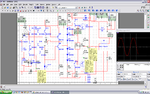
Multisim clutters its schematic by cutting wires and inserting a current meter. XWM2 has a voltmeter and a current meter, it is not a power source.
Multisim also clutters its schematic with chicken pox dots all over the place.
 
  • Like
Reactions: FvM

    FvM

    Points: 2
    Helpful Answer Positive Rating
Yeah, I thinked they know its not a power source, its a power meter.
 
Last edited:

I solved the issue this way but i wanted to fix the initial sch.
It wasnt the output stage as I mentioned because i have tested it separately.

slvd1.PNG

slvd2.PNG

slvd3.PNG

Oh now there are a lot of Power dissip. at Q1 and Q5.
 
Last edited:

You can't assume that the output stage has no contribution
just because you test it separately. The low power "op amp"
and the current demanded from it by the buffer stage and
output stage may be incompatible, leading to a less than
expected output swing. A way to test this is to buffer the
op amp section with an ideal vcvs before the PNP/NPN
buffer stage. If things change then the back-end load
matters. Similarly you could drive the back end with an
ideal vdc and see just what it takes to fully swing the
output - then move this to before the PNP/NPN buffer -
and see whether the output may work fine solo, but
need something its predecessors can't give it. Look at
the current drawn from those ideal sources, too.
 

Yes this makes sense, but i tested with BDs and a more heavy load. Same story. :thinker:

I fixed the Pd mentioned in my prev post but now i have another issue.
maybe i need some balance between 4 and 5 bias diodes. -> 4 + 2 resistors up and down.issue.PNG

- - - Updated - - -

look same with a vcvs
vcvs.PNG
 

updated sch

strang3.PNG

strang3_2.PNG

strang3_3.PNG
 

I tested the op amp from post #1 without an output stage and it actually works, but something strange happens because i tried with a ideal buffer (voltage controlled voltage source) and it was clipping.
This means its no current related, theres nothing else to cause the issue :D
Only current.
 

Why VI limiter in an amplifier clips only the bottom ?

vi.PNG :bsdetector:
 

I solved the issue, dont know only for the limiter. It looks strange to me to work only in the bottom.
HV2.PNG


There are two variants, with bootstrap+another stage or with two ccs-es instead the bootstrap without another stage :bsdetector:
 

Attachments

  • HV.PNG
    HV.PNG
    126.2 KB · Views: 69

Status
Not open for further replies.

Similar threads

Part and Inventory Search

Welcome to EDABoard.com

Sponsor

Back
Top