stackprogramer
Full Member level 3
i want to share reason why means a wafer a is 100 or 111?
from view point structure
- - - Updated - - -
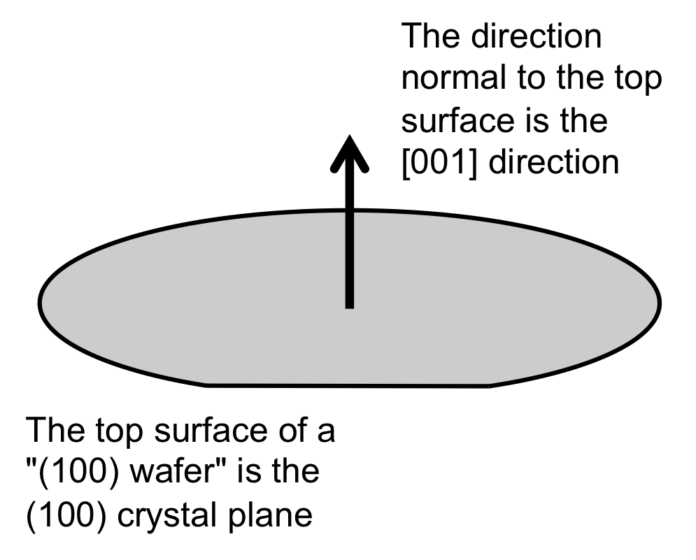
when a wafer is talked is 100 it means that vector 001 is angle to plane (100)
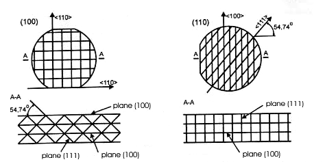
we in surface wafer we have some square that miller indice for plane we can uses for calling our wafer.
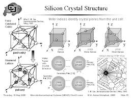
we uses this symbols for naming wafer n-type or p-type

more description in **broken link removed**
from view point structure
- - - Updated - - -
when a wafer is talked is 100 it means that vector 001 is angle to plane (100)
we in surface wafer we have some square that miller indice for plane we can uses for calling our wafer.
we uses this symbols for naming wafer n-type or p-type
more description in **broken link removed**
Last edited: