orso135
Newbie level 4
Hello! ")
I am a just-graduated engineer and right now I am doing an internship in Japan. My task is to develop a SMPTE time code decoder on a FPGA ALTERA DE0 TERASIC and display the time-code on the 7-segment displays.
I have attended two courses at the university about digital design, but up to now I have no practical experience and unfortunately my supervisor knows nothing about VHDL.
Quick summary of the theory behind the timecode:
• SMPTE timecode is a set of cooperating standards to label individual frames of video or film with a time code. Timecodes are added to film, video or audio material, and have also been adapted to synchronize music.
(Wikipedia: http://en.wikipedia.org/wiki/SMPTE_timecode )
• Timecode is encoded using LTC
(Wikipedia: http://en.wikipedia.org/wiki/Linear_timecode )
• The bits are encoded using the biphase mark code (also known as FM): a 0 bit has a single transition at the start of the bit period. A 1 bit has two transitions, at the beginning and middle of the period. This encoding is self-clocking.(http://www.philrees.co.uk/articles/timecode.htm )
This is the basic design I came up with and I would like to have your opinion about it
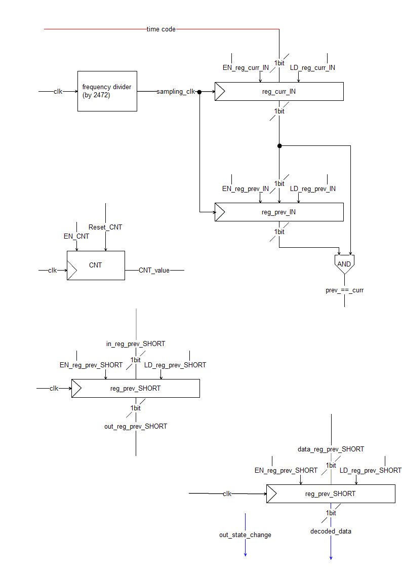
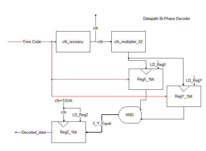
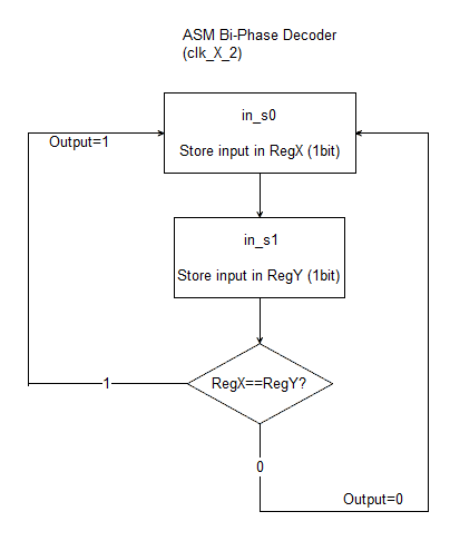
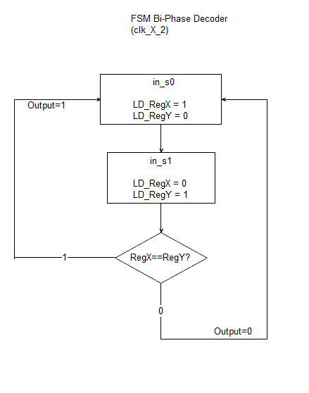
The first step is to decode the time-code (encoded in Bi-Phase Mark). In the figure below there is the data-path of the Bi-Phase decoder.
First, clock recovery has to be performed using a PLL. Then the following FSM that changes states after every clock edge (twice in a clock period) can be employed.

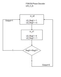
In states in_s0 and in_s1 (respectively first and second half periods) the input is saved in RegX and RegY (both 1 bit registers). The stored values are then compared, if:
• they are equal then the decoded value is a ‘0’
• they are different then the decoded value is a ‘1’
At the following clock edge the current state is restored to state in_s0. The value of the two registers is compared and with an offset of half period the result is saved in a register (RegZ) that holds it for a whole clock period.
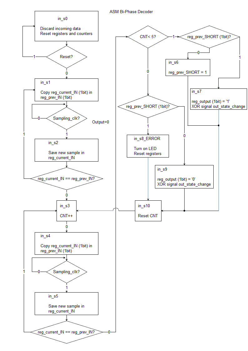
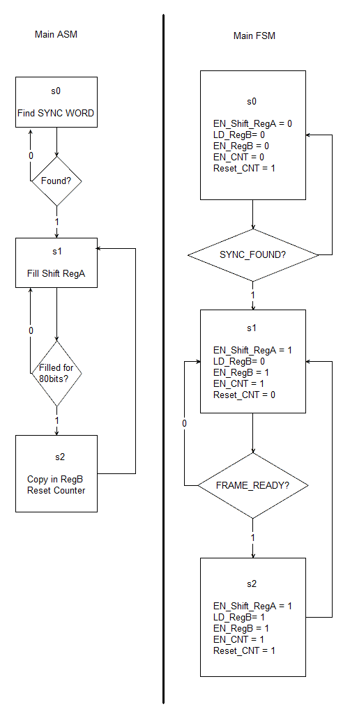
Below there is the Algorithm State Machine and Finite State Machine of the main design.
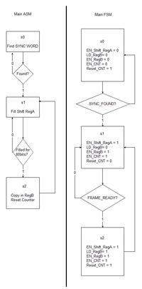
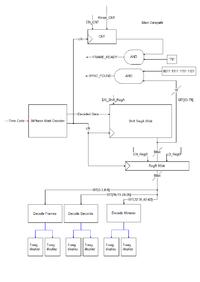
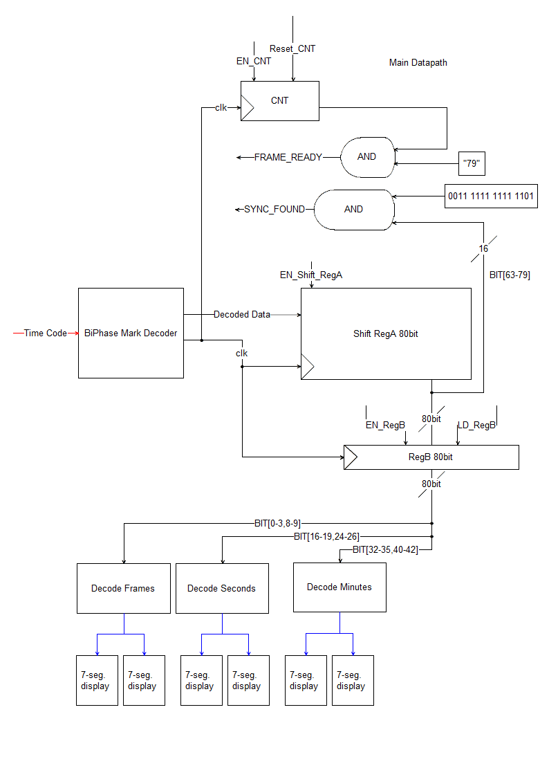
Once the clock has been recovered and the time code decoded then the shift register A (regA) is filled.
The last 16 bits are constantly compared with the SYNC WORD. This is accomplished in the state s0 (new FSM see attachment 5).
Once the SYNC WORD has been found then the FSM jumps to state s1 where a counter that was initially set to 0 is now enabled. When the counter reaches 79 (that is 80 clock ticks starting from 0) then the state becomes s2 (that is the whole timecode frame of 80bit has been saved).
In state s2 the timecode frame (80bits) is copied into the register B (regB) and the counter is now reset.
The combinatorial decoders (for frames, seconds and minutes) make sure that the correct bits inside the timecode frame are correctly displayed using the 7-segment displays of the DE0 board.
My questions are the following:
• How would you accomplish clock recovery on an FPGA? I previously found this https://www.edaboard.com/threads/11258/, but I did not really understood it. Do you have any suggestions?
• Does the Bi-Phase decoding algorithm make sense to you or you would employ another (maybe easier) solution?
• Do you think this design is feasible? Do you see any flaws or possible improvements that can be made?
Any comment is highly appreciated! Thank you very much for your support!
I am a just-graduated engineer and right now I am doing an internship in Japan. My task is to develop a SMPTE time code decoder on a FPGA ALTERA DE0 TERASIC and display the time-code on the 7-segment displays.
I have attended two courses at the university about digital design, but up to now I have no practical experience and unfortunately my supervisor knows nothing about VHDL.
Quick summary of the theory behind the timecode:
• SMPTE timecode is a set of cooperating standards to label individual frames of video or film with a time code. Timecodes are added to film, video or audio material, and have also been adapted to synchronize music.
(Wikipedia: http://en.wikipedia.org/wiki/SMPTE_timecode )
• Timecode is encoded using LTC
(Wikipedia: http://en.wikipedia.org/wiki/Linear_timecode )
• The bits are encoded using the biphase mark code (also known as FM): a 0 bit has a single transition at the start of the bit period. A 1 bit has two transitions, at the beginning and middle of the period. This encoding is self-clocking.(http://www.philrees.co.uk/articles/timecode.htm )
This is the basic design I came up with and I would like to have your opinion about it
The first step is to decode the time-code (encoded in Bi-Phase Mark). In the figure below there is the data-path of the Bi-Phase decoder.
First, clock recovery has to be performed using a PLL. Then the following FSM that changes states after every clock edge (twice in a clock period) can be employed.
In states in_s0 and in_s1 (respectively first and second half periods) the input is saved in RegX and RegY (both 1 bit registers). The stored values are then compared, if:
• they are equal then the decoded value is a ‘0’
• they are different then the decoded value is a ‘1’
At the following clock edge the current state is restored to state in_s0. The value of the two registers is compared and with an offset of half period the result is saved in a register (RegZ) that holds it for a whole clock period.
Below there is the Algorithm State Machine and Finite State Machine of the main design.
Once the clock has been recovered and the time code decoded then the shift register A (regA) is filled.
The last 16 bits are constantly compared with the SYNC WORD. This is accomplished in the state s0 (new FSM see attachment 5).
Once the SYNC WORD has been found then the FSM jumps to state s1 where a counter that was initially set to 0 is now enabled. When the counter reaches 79 (that is 80 clock ticks starting from 0) then the state becomes s2 (that is the whole timecode frame of 80bit has been saved).
In state s2 the timecode frame (80bits) is copied into the register B (regB) and the counter is now reset.
The combinatorial decoders (for frames, seconds and minutes) make sure that the correct bits inside the timecode frame are correctly displayed using the 7-segment displays of the DE0 board.
My questions are the following:
• How would you accomplish clock recovery on an FPGA? I previously found this https://www.edaboard.com/threads/11258/, but I did not really understood it. Do you have any suggestions?
• Does the Bi-Phase decoding algorithm make sense to you or you would employ another (maybe easier) solution?
• Do you think this design is feasible? Do you see any flaws or possible improvements that can be made?
Any comment is highly appreciated! Thank you very much for your support!
Last edited by a moderator: