jutlwj
Newbie level 6
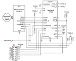
I am trying to design a PCB with Spartan 6 FT(G)256 Package and it will be configured by EZ-USB FX2 CY7C68013A. The configuration mode will be Microprocessor-Driven SelectMAP Configuration, as shown in the attached image and what is described in the following document:
https://www.xilinx.com/support/documentation/user_guides/ug380.pdf
My confusion is about the data bus connection. On FX2 side, the data bus is FD[15..0], on Spartan 6 side, the data bus is D[15..0]. As you know, D0 is the pin IO_L3P_D0_DIN_MISO_MISO1_2, D1 is the pin IO_L12P_D1_MISO2_2, D2 the pin IO_L12N_D2_MISO3_2 ..... D15 is the pin IO_L31N_GCLK30_D15_2. I take it for granted that data pin on FX2 side should be connected to the data pin on Spartan 6 side which is at the same position in the data bus of Spartan 6. That is to say, FD0 of FX2 should be connected to D0 of Spartan 6, FD1 of FX2 to D1of Spartan 6, FD2 to D2, FD3 to D3......FD15 to D15. This is my understanding.
I have an similar PCB of earlier version designed by other people, which is my design reference at the moment. On that PCB, all other signals required in the configuration are the same apart from the data bus connection. On that PCB, FD0 of FX2 was connected to D12 of Spartan 6, FD1 of FX2 connected to D11 of Spartan 6, FD2 to D0, FD3 to D10, FD4 to D4, FD5 to D6,FD7 to D1, FD8 to D13, FD9 to D14, FD10 to D15, FD11 to D8, FD12 to D9, FD13 to D4, FD14 to D7, FD15 to D3. You can see, it looks that the data lines are connected in a messy corresponding sequence. But what makes me very confused is that PCB still works! Programming the Spartan 6 through FX2 has always been successful. It should not have been working. Could anybody please explain to me why this messy connection sequence still works in the configuration of Spartan 6? I can connect FD0 to D0, FD1 to D1....FD15 to D15, but the design on that reference board really makes me confused. Is there anything I missed in understanding this?

Last edited: