Continue to Site

Welcome to EDAboard.com

Welcome to our site! EDAboard.com is an international Electronics Discussion Forum focused on EDA software, circuits, schematics, books, theory, papers, asic, pld, 8051, DSP, Network, RF, Analog Design, PCB, Service Manuals... and a whole lot more! To participate you need to register. Registration is free. Click here to register now.

[SOLVED] Can't fit design in device - error with pins

Status
Not open for further replies.

preethi19

Full Member level 5
Joined
Jun 30, 2014
Messages
273
Helped
0
Reputation
0
Reaction score
1
Trophy points
16
Activity points
3,474
Cant fit design in device - error re pins

Hi i am learning about working with FPGA's and i am trying a simple or gate logic. Following is the code
Code:
library ieee;
use ieee.std_logic_1164.all;

--ENTITY DECLARATION: name, inputs, outputs
entity orGate is
   port( A, B : in std_logic;
            F : out std_logic);
end orGate;

--FUNCTIONAL DESCRIPTION: how the OR Gate works
architecture func of orGate is 
begin
   F <= A or B;
end func;


I somehow managed to assign the pins to the inputs and output of the or gate. After assigning the pin location when i run "start I/O assignment analysis", i am getting an error saying "can't fit design in device". I read the cause of this problem and it was posted that there might be error in source code. But after writing the VHDL code when i run compilation i dont get any errors and it is successful. But after assigning pins when i do that it is failing. I assigned the pins according to the kits manual for the FPGA pins. Can anyone please help me out with this problem. Thank you!!!
 
Last edited:
Re: Cant fit design in device - error re pins

Post the SDC file that has the pin assignments. It's most likely a problem with assigning a pin that is not allowed.
 

Re: Cant fit design in device - error re pins

Thank you for the reply!!! I was able to correct the error. I was able to find the appropriate pins for all the inputs and outputs. And even the programmer section is successfully. But the or gate logic is not working. No LED turns on when i push any button to give the two inputs. Also i couldn't find any SDC file. Any help pls!!! I used the following pdf file for pin reference. Please check pins F1 and F2 for inputs and P12 for output.

 
Last edited:

Re: Cant fit design in device - error re pins

Hi,

Maybe a hardware problem. Did you properly use pullup/pulldown at the buttons?

Klaus
 

Re: Cant fit design in device - error re pins

Could you kindly elaborate on the "pullup and pulldown at the buttons". I assume that pullup is assuming to hold the logic to high ie 1 and pulldown is gnd that is logic 0. pls correct me if i'm wrong abt this. But i don't get any option wer i can choose logic 1 and logic 0. I just have an option "reserved" wer it gives allows me to choose between
1. As bidirectional
2. As input tristated
3. As output driving VCC etc.
And as far as the hardware is concerned i don't think it must be an issue becoz this kit was previously used by one of the students. Thank you!!!

- - - Updated - - -

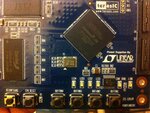
I have attached an image of the kit i have. Also an image of the manual it came with that describes about the assigned FPGA pins. This manual didn't have pin description for the LEDs. So i had to find a pin file manually which in this post i have attached as a pdf file from where i was able to obtain the pin for LED. I have provided the main information. Rest is simple VHDL code and compilation steps only. I am assuming this is the part wer i am making some mistake. It would be really helpful if anyone could give any suggestions. Thank you all for the replies so far!!! :)

image (1).jpeg

image (2).jpeg

I also tried changing the pins too. Didn't still work

pin assign.png

sch.png
 

Re: Cant fit design in device - error re pins

Hi,

Post the schematic how the buttons are connected to the Fpga.

How is it made to be valid high and low levels?

The picture if the pcb doesn't help.

Klaus
 

Re: Cant fit design in device - error re pins

I see that you connected valid KEY and LED pins in your minimal design. It should work without further prerequisites, all necessary assignments are derived from the schematic.

But I guess you overlooked that keys and LEDs have both active low polarity. Need to push both buttons to light the LED in case of an OR gate. Or you didn't yet manage to download your compiled design to the FPGA.

Did you notice the tutorials provided with the board documents. Performing "My first FPGA design" should touch all the problems you are asking about.
 
Re: Cant fit design in device - error re pins

Thank you so much!!! Its working now. As you told i just kept pushing the buttons and left a hold of them. Now by keeping on holding the buttons i am able to see the LED logic glow. But just one doubt. Its OR gate logic. So when either one of the buttons is held high the output (LED) should be on. But the output logic is only ON when i keep pressing both the input buttons to logic 1. When i press just any one of the input then there is no output. Can anyone kindly let me know why is this. And its not like wer i wrote a VHDL code too for it to be wrong. I just created a block diagram and just used an OR gate from the library. and just gave input output pins and assigned them to the FPGA pins. So no possibility of error in logic is likely to occur right. Thanks again!!! :)
 

Re: Cant fit design in device - error re pins

As said, keys and LEDs have inverted polarity. You can reflect this by using an AND instead of an OR gate. Or add inverters for in and outputs.
 
Re: Cant fit design in device - error re pins

The pins use active low logic, i.e. negative logic.

Therefore...using A & B as inputs and X as the output

Buttons drive a 0 on A & B when pressed (i.e. active-low) and the LED output pin, X, is active when the pin is driven low (i.e. active-low).

High/low voltage wise we have
A B | X
0 0 | 0 - output is active (active low)
0 1 | 1 - output is inactive
1 0 | 1 - output is inactive
1 1 | 1 - output is inactive

logically this means
A B | X
T T | T - True logic level
T F | F - False logic level
F T | F - False logic level
F F | F - False logic level

As you can see the OR gate with inversions on the inputs and outputs behaves like an AND gate.
Using DeMorgan's Theorem...
A & B => !(!A + !B), i.e. invert the OR gate inputs and the OR gate output makes an AND gate see this.
 

Status
Not open for further replies.

Similar threads

Part and Inventory Search

Welcome to EDABoard.com

Sponsor

Back
Top