Continue to Site

Welcome to EDAboard.com

Welcome to our site! EDAboard.com is an international Electronics Discussion Forum focused on EDA software, circuits, schematics, books, theory, papers, asic, pld, 8051, DSP, Network, RF, Analog Design, PCB, Service Manuals... and a whole lot more! To participate you need to register. Registration is free. Click here to register now.

High side driver with no current infusion to source?

Status
Not open for further replies.

kanonka

Member level 1
Joined
Dec 12, 2011
Messages
35
Helped
0
Reputation
0
Reaction score
0
Trophy points
1,286
Activity points
1,760
Hi, I need some help on the high side driver idea/part/schematic.

I need to drive high-side mosfets in H-Bridge config AND precisely measure current that goes into the load. Originally I did it very simple way: V+ goes to current sensing resitor, then goes H-Bridge. Problem is that my V+ is 43V, so I somehow need to clamp voltage on a high side gates. I did it standard way - added Zener diodes. Problem with this approach is that Zener diode sends some additional current to the load, which my sensing resistor does not measure.

So, if there any way to drive high side mosfet without affecting current on the load? (well, effect of 1uA or less would be acceptable). Let me rephrase that: yes, I know it's possible -just add op amp to measure voltage off the corresponding side of the load, and then just use that voltage as a ref for high side driver, but this adds too much of a complexity to the design. So, is there a simple way?

Another possibility is to add current sensing resistor right before the load, but this will require bidirectional current sensing op amp + some circuit to take an "absolute" value from the result, which is even more complicated.

Any ideas?
 

How about a low-side shunt?

The voltage clamp point isn't clear, you should clarify your gate driver configuration.
 

If I have low-side shunt, I would not be able to detect short-circuit, so that goes out of question.

Voltage clump point is simple: I have Zener (15V) connected between gate and source. Gate is connected to a simple mosfet switch (powered from a separate voltage of +49V, so I have 6V to fully open my H-Bridge high side mosfet). If my +43V driving voltage for a bridge would stay permanent, this would be no problem then: source is either at ~+43V and gate at +49V (6V difference), or source is at ground together with gate (~0V difference). But my +43V can go anywhere between +43V and zero. So, when high side mosfet is on (gate at +49V), source can be, for example, at +15V. So, this difference needs to be clamped. Zener does clamp perfectly, except it starts to infuse current into the load; this current is taken from +49V rail of driving mosfet, goes into the load via Zener, and bypasses my current sensing resistor. I can reduce this extra current by increasing resistor between +49V rail and drain of driving mosfet, but a) it will never be small enough and b) this will reduce switching time.

It is also my understanding, that most (all?) high side driver IC use Zener clamps in this exact config, so this would not solve the issue. Or are there any IC that use different approach?
 
Last edited:

If I have low-side shunt, I would not be able to detect short-circuit, so that goes out of question.

You are apparently referring to unsaid prerequisites, e.g. DC- connected to chassis ground etc. Not generally valid for H-bridges.

I believe there are possible solutions, e.g. clamp the gate voltage to the output of a simple buffer (complementary emitter follower) instead directly to bridge center. But a detail solution should refer to a more exact specification.
 
Yeah! Didn't think about such a simple thing! Thanks! Simple source follower will solve it! Now, is there simple way to get rid of the gate-source capacitance of the follower that it adds to the scene? Or at least reduce it to insignificant numbers?
 

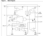
There are plenty of High Side switches with short cct protection. 50V

Here's one albeit long leadtime $2.20,
image.jpg
 

Ok, seems like I still have a problem.

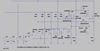
To clarify, here is my circuit (was unable to attach .asc file for LTSpice, so here is it's content):
Code:
Version 4
SHEET 1 880 680
WIRE -768 -496 -1216 -496
WIRE -432 -496 -768 -496
WIRE -128 -496 -432 -496
WIRE 176 -496 -128 -496
WIRE -32 -448 -1104 -448
WIRE -32 -432 -32 -448
WIRE -32 -336 -32 -352
WIRE -32 -336 -208 -336
WIRE 96 -336 -32 -336
WIRE -208 -320 -208 -336
WIRE 96 -320 96 -336
WIRE -656 -304 -1328 -304
WIRE -544 -304 -656 -304
WIRE -336 -304 -544 -304
WIRE -768 -288 -768 -496
WIRE -656 -288 -656 -304
WIRE -544 -288 -544 -304
WIRE -432 -288 -432 -496
WIRE -336 -288 -336 -304
WIRE -128 -288 -128 -496
WIRE 176 -272 176 -496
WIRE -256 -240 -304 -240
WIRE 48 -240 -32 -240
WIRE -208 -208 -208 -224
WIRE -176 -208 -208 -208
WIRE -432 -192 -432 -208
WIRE -304 -192 -304 -240
WIRE -304 -192 -432 -192
WIRE -288 -192 -304 -192
WIRE -128 -192 -224 -192
WIRE 96 -192 96 -224
WIRE 128 -192 96 -192
WIRE -768 -144 -768 -208
WIRE -32 -144 -32 -240
WIRE -32 -144 -768 -144
WIRE 0 -144 -32 -144
WIRE 176 -144 176 -176
WIRE 176 -144 64 -144
WIRE -208 -64 -208 -208
WIRE -32 -64 -208 -64
WIRE 96 -64 96 -192
WIRE 96 -64 48 -64
WIRE -656 -32 -656 -208
WIRE -272 -32 -656 -32
WIRE -208 -32 -208 -64
WIRE -544 -16 -544 -208
WIRE -496 -16 -544 -16
WIRE -400 -16 -496 -16
WIRE -336 -16 -336 -208
WIRE -288 -16 -336 -16
WIRE -768 0 -768 -144
WIRE -656 0 -656 -32
WIRE -544 0 -544 -16
WIRE -432 0 -432 -192
WIRE -336 0 -336 -16
WIRE 96 0 96 -64
WIRE -272 48 -272 -32
WIRE -256 48 -272 48
WIRE -960 80 -1008 80
WIRE -864 80 -880 80
WIRE -816 80 -864 80
WIRE -704 80 -720 80
WIRE -592 80 -608 80
WIRE -496 80 -496 -16
WIRE -480 80 -496 80
WIRE -400 80 -400 -16
WIRE -384 80 -400 80
WIRE -288 80 -288 -16
WIRE 48 80 -288 80
WIRE -1328 112 -1328 -304
WIRE -1216 112 -1216 -496
WIRE -1104 112 -1104 -448
WIRE -1008 112 -1008 80
WIRE -128 112 -128 -192
WIRE 176 112 176 -144
WIRE -864 144 -864 80
WIRE -720 144 -720 80
WIRE -720 144 -864 144
WIRE -608 144 -608 80
WIRE -608 144 -720 144
WIRE -1328 224 -1328 192
WIRE -1216 224 -1216 192
WIRE -1216 224 -1328 224
WIRE -1104 224 -1104 192
WIRE -1104 224 -1216 224
WIRE -1008 224 -1008 192
WIRE -1008 224 -1104 224
WIRE -768 224 -768 96
WIRE -768 224 -1008 224
WIRE -656 224 -656 96
WIRE -656 224 -768 224
WIRE -544 224 -544 96
WIRE -544 224 -656 224
WIRE -432 224 -432 96
WIRE -432 224 -544 224
WIRE -336 224 -336 96
WIRE -336 224 -432 224
WIRE -208 224 -208 64
WIRE -208 224 -336 224
WIRE -128 224 -128 192
WIRE -128 224 -208 224
WIRE 96 224 96 96
WIRE 96 224 -128 224
WIRE 176 224 176 192
WIRE 176 224 96 224
WIRE -1328 240 -1328 224
FLAG -1328 240 0
SYMBOL res -48 -448 R0
SYMATTR InstName Rsense
SYMATTR Value 10
SYMBOL nmos -256 -320 R0
WINDOW 3 -69 -8 Left 2
WINDOW 0 57 2 Left 2
SYMATTR Value Si4850EY
SYMATTR InstName M1
SYMBOL res -352 -304 R0
WINDOW 0 -41 34 Left 2
WINDOW 3 -45 69 Left 2
SYMATTR InstName R6
SYMATTR Value 40k
SYMBOL nmos -384 0 R0
WINDOW 0 9 109 Left 2
WINDOW 3 -41 136 Left 2
SYMATTR InstName M2
SYMATTR Value 2N7002
SYMBOL nmos -480 0 R0
WINDOW 0 -3 101 Left 2
WINDOW 3 -42 126 Left 2
SYMATTR InstName M3
SYMATTR Value 2N7002
SYMBOL res -416 -192 R180
WINDOW 0 36 76 Left 2
WINDOW 3 36 40 Left 2
SYMATTR InstName R7
SYMATTR Value 40k
SYMBOL res -640 -192 R180
WINDOW 0 36 76 Left 2
WINDOW 3 36 40 Left 2
SYMATTR InstName R8
SYMATTR Value 40k
SYMBOL nmos -704 0 R0
WINDOW 0 -52 22 Left 2
WINDOW 3 -48 -11 Left 2
SYMATTR InstName M4
SYMATTR Value 2N7002
SYMBOL nmos -816 0 R0
WINDOW 0 -43 28 Left 2
WINDOW 3 -42 -7 Left 2
SYMATTR InstName M5
SYMATTR Value 2N7002
SYMBOL res -752 -192 R180
WINDOW 0 36 76 Left 2
WINDOW 3 36 40 Left 2
SYMATTR InstName R9
SYMATTR Value 40k
SYMBOL voltage -1008 96 R0
WINDOW 3 28 96 Left 2
WINDOW 123 0 0 Left 2
WINDOW 39 0 0 Left 2
SYMATTR Value 3.3
SYMATTR InstName V1
SYMBOL res -864 64 R90
WINDOW 0 0 56 VBottom 2
WINDOW 3 32 56 VTop 2
SYMATTR InstName R10
SYMATTR Value 1k
SYMBOL zener 64 -160 R90
WINDOW 0 1 67 VBottom 2
WINDOW 3 36 43 VTop 2
SYMATTR InstName D1
SYMATTR Value BZX84C6V2L
SYMATTR Description Diode
SYMATTR Type diode
SYMBOL res 64 -80 R90
WINDOW 0 58 108 VBottom 2
WINDOW 3 31 16 VTop 2
SYMATTR InstName Rload
SYMATTR Value 500
SYMBOL nmos 48 -320 R0
WINDOW 0 -35 1 Left 2
WINDOW 3 -104 33 Left 2
SYMATTR InstName M6
SYMATTR Value Si4850EY
SYMBOL nmos 48 0 R0
WINDOW 0 -36 1 Left 2
WINDOW 3 -106 29 Left 2
SYMATTR InstName M7
SYMATTR Value Si4850EY
SYMBOL nmos -256 -32 R0
WINDOW 0 -14 129 Left 2
WINDOW 3 -64 159 Left 2
SYMATTR InstName M8
SYMATTR Value Si4850EY
SYMBOL nmos -592 0 R0
WINDOW 0 -52 24 Left 2
WINDOW 3 -51 -7 Left 2
SYMATTR InstName M9
SYMATTR Value 2N7002
SYMBOL res -528 -192 R180
WINDOW 0 36 76 Left 2
WINDOW 3 36 40 Left 2
SYMATTR InstName R11
SYMATTR Value 40k
SYMBOL zener -224 -208 R90
WINDOW 0 -1 57 VBottom 2
WINDOW 3 37 49 VTop 2
SYMATTR InstName D2
SYMATTR Value BZX84C6V2L
SYMATTR Description Diode
SYMATTR Type diode
SYMBOL nmos 128 -272 R0
WINDOW 0 58 -6 Left 2
WINDOW 3 53 30 Left 2
SYMATTR InstName M10
SYMATTR Value 2N7002
SYMBOL res 160 96 R0
WINDOW 0 -41 34 Left 2
WINDOW 3 -33 84 Left 2
SYMATTR InstName R12
SYMATTR Value 10k
SYMBOL nmos -176 -288 R0
WINDOW 0 52 54 Left 2
WINDOW 3 55 85 Left 2
SYMATTR InstName M11
SYMATTR Value 2N7002
SYMBOL res -144 96 R0
WINDOW 0 -41 34 Left 2
WINDOW 3 -33 84 Left 2
SYMATTR InstName R13
SYMATTR Value 10k
SYMBOL voltage -1104 96 R0
WINDOW 3 -14 195 Left 2
WINDOW 123 0 0 Left 2
WINDOW 39 0 0 Left 2
SYMATTR Value PULSE(0 40 0 0.000001 0.000001 0.0005 0.001 10)
SYMATTR InstName V2
SYMBOL voltage -1216 96 R0
WINDOW 3 28 96 Left 2
WINDOW 123 0 0 Left 2
WINDOW 39 0 0 Left 2
SYMATTR Value 45
SYMATTR InstName V3
SYMBOL voltage -1328 96 R0
WINDOW 3 28 96 Left 2
WINDOW 123 0 0 Left 2
WINDOW 39 0 0 Left 2
SYMATTR Value 19.5
SYMATTR InstName V4
TEXT -1360 312 Left 2 !.tran 0.01
And here is the image:


Problem is that this circuit should be able to handle Rload from 500 Ohm to 2Mohm. If you'll take a look at current that runs by Rsense, you'll notice that is has spikes at turn on/off moments. I can tolerate them when load is ~500 Ohm, but at already 5k they will screw up all measuring. Also, if you change V2 from pulse to sine, you'll notice that with Rload = 10K current amplitudes on Rsense and Rload start to differ for about 1%; with Rload = 100K current through Rsense becomes basically unreadable.

Any advice?
 
Last edited by a moderator:

Status
Not open for further replies.

Part and Inventory Search

Welcome to EDABoard.com

Sponsor

Back
Top