Continue to Site

Welcome to EDAboard.com

Welcome to our site! EDAboard.com is an international Electronics Discussion Forum focused on EDA software, circuits, schematics, books, theory, papers, asic, pld, 8051, DSP, Network, RF, Analog Design, PCB, Service Manuals... and a whole lot more! To participate you need to register. Registration is free. Click here to register now.

Can a ground plane on another layer replace a guard trace?

Status
Not open for further replies.

randomshinichi

Newbie level 6
Joined
Jul 23, 2013
Messages
13
Helped
0
Reputation
0
Reaction score
0
Trophy points
1
Activity points
164
I've been reworking my PCB so that the ground plane on the top layer (with all the critical signals) can reach between traces more of the time, effectively having the guard trace accompany the signal trace as long as possible. The question is, the other side of my PCB is mostly a contiguous ground plane, so is this really necessary?
 

Like everything, I think it depends. A guard trace may help prevent an adjacent trace on the same layer from causing interface; ground plane beneath the traces may not have as good an effect.
 

the crosstalk can be estimated by the ratio of coupling capacitance/impedance to line capacitance/impedance.

How much crosstalk is acceptable? Are they synchronous bus signals or async?
If sync then tolerance to crosstalk is high, Otherwise, crosstalk needs to be less than noise margin or < 25% or so. determined by geometry of gap and thickness to ground.
 

I think "guard trace" isn't but an umbrella term for different layout features. As far as capacitive cross-talk is addressed, you can calculate the actual mutual capacitance of the involved nets. For highest isolation, both ground plane and coplanar guard traces, possibly with via fences, might be reasonable.
 

View attachment auteur201.zip
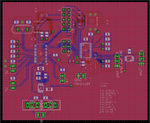
Well, here's my design. It looks like this:
yup.png

Introduction: A very sensitive, low amplitude signal comes in through 0, gets amplified by an instrumentation amplifier, and goes into the ADC (CHAN1_N, CHAN1_P). It is imperative that as little noise reaches channel 0 as possible. Other channels are unused and the headers and lines are just there for fun.

1. The ground plane accompanies the input signal's traces for as long as it can, but would it do just as well without the ground plane right next to these traces? Because of REF0, the ground plane cannot accompany CHAN1_N near the ADC's pin, although CHAN1_P is accompanied. What does this mean for the signal quality?

2. SPI is handled by the six pin connector at the middle of the board, and goes into the ADC (left) and DAC (right). SPI-DIN is in the middle. The other SPI lines have the ground plane guarding them on the sides, but the DIN line has no such luxury. Is this going to be a problem? I think it'll run about 20MHz max.

3. For a guard trace/ground plane to be effective, does it have to be between the traces which have to be isolated from one another? I can't just put the guard trace on one side and hope that the trace concentrates all its interference there and ignores the other trace next to it? What happens if there isn't any space (like in the case of SPI-DIN), am I fubar? I see lots of traces on a AGP video card without the ground plane next to them, they seem to work fine. Am I overthinking this?

3. The ADC's crystal (24.576MHz) has one line that doesn't have space for the ground plane next to it (N$16). Will it somehow disturb the other lines, especially the 3V3-SUPPLY line that runs right next to it? Should I worry about that?

4. Is capacitive cross talk what I should be worried about here? Or are there bigger problems? The goal of the design is to have as little noise on ADC's channel 0 as possible, while having the SPI interface run as fast as possible.

Extra question: The signal 2.5V-REFERENCE - in order to prevent voltage drop across the trace, the trace is made as wide as possible (can I make that trace specifically of a different thickness?), but thanks to clearance issues, I can't really do that at the pin. If the trace near the pin can only be 10 mils wide, does it make still sense for the rest of the trace to be wider?
 
Last edited:

Since you have both analog and digital signals it would be best that the ground be split to generate a separate analog and digital ground with analog signals confined to the analog ground plane and digital signals confined to the digital ground plane. The planes should be tied together at one spot (usually near or under the ADC). A surface-mount ferrite bead for this connection can be used to improve high frequency isolation between the two planes. Keep the digital signals as far from the sensitive analog signals as possible.
 

Status
Not open for further replies.

Similar threads

Part and Inventory Search

Welcome to EDABoard.com

Sponsor

Back
Top