ashyma
Newbie level 6
I have a major problem and i am out of ideas so any suggestions will be great....
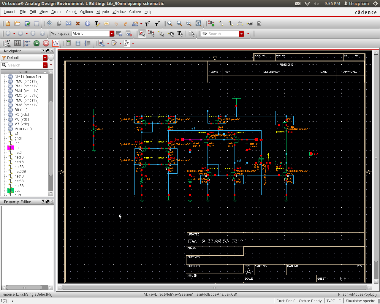
below is the image of the circuit i am trying to simulate: its for an OTA using 90nm technology: the requirements are
1. high linearity 2. high gain 3.low noise... the only difference in my circuit from the one in the image is that i am using all PMOSs
1) https://obrazki.elektroda.pl/3237069900_1362096134.jpg
This the linearity curve i am getting:
2)https://obrazki.elektroda.pl/3452880100_1362096357.jpg
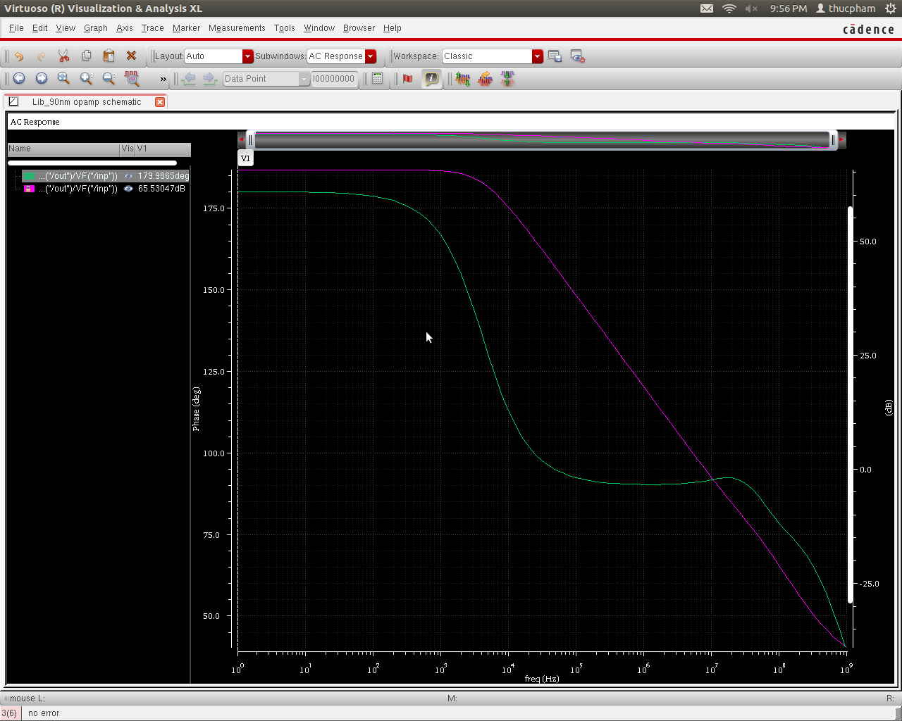
and i am getting a very bad curve for the gain as shown below:
https://obrazki.elektroda.pl/7154024700_1362096444.jpg
I chose the Ibias to be 4uA... the aspect ratios are as follows:
for M1&M2 are W=8.769n L=90nm
for M3 to M6 are W=5.35u L=180nm
for M7 & M8 are W=2.67u L=180nm
for M9 & M10 are W=8.769nm L=90nm
for Mcascp are W=450n L=1.35u
for Mcascn are W=7.35u L=1.35u
I dnt know whats the problem... the curve for the linearity looks ok.. but the gain is so bad.. i dont knw how to fix this from where to do i start ... so any suggestions are highly appreciated..
Thanks in advance
below is the image of the circuit i am trying to simulate: its for an OTA using 90nm technology: the requirements are
1. high linearity 2. high gain 3.low noise... the only difference in my circuit from the one in the image is that i am using all PMOSs
1) https://obrazki.elektroda.pl/3237069900_1362096134.jpg
This the linearity curve i am getting:
2)https://obrazki.elektroda.pl/3452880100_1362096357.jpg
and i am getting a very bad curve for the gain as shown below:
https://obrazki.elektroda.pl/7154024700_1362096444.jpg
I chose the Ibias to be 4uA... the aspect ratios are as follows:
for M1&M2 are W=8.769n L=90nm
for M3 to M6 are W=5.35u L=180nm
for M7 & M8 are W=2.67u L=180nm
for M9 & M10 are W=8.769nm L=90nm
for Mcascp are W=450n L=1.35u
for Mcascn are W=7.35u L=1.35u
I dnt know whats the problem... the curve for the linearity looks ok.. but the gain is so bad.. i dont knw how to fix this from where to do i start ... so any suggestions are highly appreciated..
Thanks in advance