Continue to Site

Welcome to EDAboard.com

Welcome to our site! EDAboard.com is an international Electronics Discussion Forum focused on EDA software, circuits, schematics, books, theory, papers, asic, pld, 8051, DSP, Network, RF, Analog Design, PCB, Service Manuals... and a whole lot more! To participate you need to register. Registration is free. Click here to register now.

[SOLVED] [MOVED] Adding separate solder mask layer in PADS

Status
Not open for further replies.

cjrathi

Member level 2
Joined
Oct 18, 2012
Messages
52
Helped
0
Reputation
0
Reaction score
0
Trophy points
1,286
Activity points
1,704
Hi,
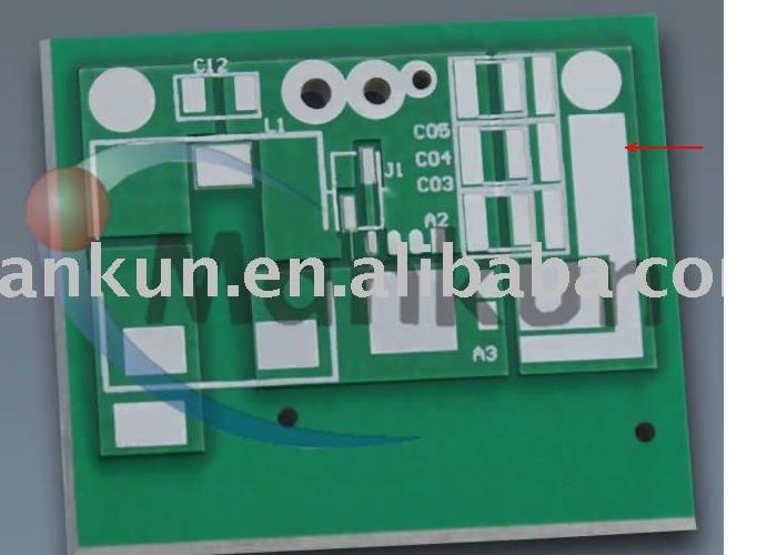
In PADS, I have separately added solder mask on top layer (of type copper) at all four edges of PCB to solder PCB to the metal body outside.
At the PCB edge there is also a pad for SMA connector.
My question is :- Does adding such type of solder mask layer mean that it is shorted to this pad of SMA connector.? (Pls see attachment for this)

In PADS, what does 'type copper' mean while adding solder mask layer ?


Solder MAsk Top layer at PCB edge.jpgTop layer at PCB edge.jpg
 

Attachments

  • Solder MAsk Top layer at PCB edge.bmp
    764.6 KB · Views: 113
  • Top layer at PCB edge.bmp
    494.9 KB · Views: 125

Hi,
you have assign the soldermask in soldermask layer only.if you assign the copper in top layer it is not a soldermask ,it is copper in top only
 

I doubt a solder mask layer to be of copper as it defies the actual purpose of solder mask it would then be no different than top layer copper..... better read out the description of "type Copper" option either in software manual or help
 

I doubt a solder mask layer to be of copper as it defies the actual purpose of solder mask it would then be no different than top layer copper..... better read out the description of "type Copper" option either in software manual or help


Really man. I didn't understand what this 'type copper' mean ? I am afraid if this is real copper, because i have already given board for fabrication.

- - - Updated - - -

Hi,
you have assign the soldermask in soldermask layer only.if you assign the copper in top layer it is not a soldermask ,it is copper in top only

Yes man. I have assigned it in solder mask top layer only. But in the field 'type', I selected copper. Do you know what does it mean ?
 

can you send top and soldermask layer PDF ,then only i come to know, you applied copper in soldermask layer right, so you opened soldermask layer


Hi rathi,
if you applied that copper in soldermask it will come like that only as i mention in red arrow mark.(fully copper will come)


Hi rathi,
if you applied that copper in soldermask it will come like that only as i mention in red arrow mark.(fully copper will come)


But what will happen at SMA connector's pad which is also at PCB edge..? I have put copper cut-out near this SMA pad.. Will this solder mask copper get short with the pad..?
 

HI
please mention in SMA connector and cut-out i could not see better mention in JPEG or PDF
 

Status
Not open for further replies.

Part and Inventory Search

Welcome to EDABoard.com

Sponsor

Back
Top